 English
 中文
 english


XC7K160T-2FFG676C is a commercial-temperature AMD Kintex-7 FPGA with 162,240 logic cells, 600 DSP48E1 slices, 11,700 Kb of block RAM, eight GTX transceivers, and up to 400 user I/O in the FFG676 package. Its mix of parallel logic, on-chip memory, signal-processing resources, and high-speed links suits designs that need several of those functions in one device.
Before specifying or buying the part, confirm two things independently. The FPGA must fit the design, and the offered material must meet the required quantity, lot, packaging, delivery, and inspection terms. A technically suitable device can still be the wrong purchase if those commercial details do not match the order.
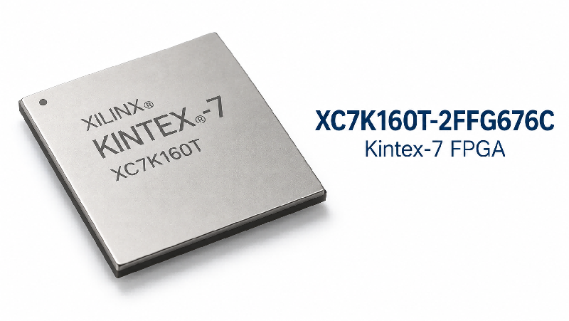
What Does the XC7K160T-2FFG676C Part Number Mean?
Every field in XC7K160T-2FFG676C identifies an orderable characteristic. Together, the fields specify the device, speed grade, package construction, environmental designation, ball count, and temperature grade.
| Code | Meaning |
|---|---|
| XC7K160T | Kintex-7 device family and XC7K160T density member |
| -2 | Standard -2 speed grade using the 1.0 V core condition |
| FF | Flip-chip fine-pitch BGA package family |
| G | RoHS 6/6 package designation with Exemption 15 |
| 676 | Package ball count, not the number of user I/O |
| C | Commercial grade with a 0°C to +85°C junction-temperature range |
Keep the complete order code on the BOM and RFQ. Dropping or changing a suffix can point to a different speed grade, package, or temperature range.
What Are the Specifications of XC7K160T-2FFG676C?
XC7K160T supplies the logic, memory, DSP, clocking, and PCIe resources, while the FFG676 package determines the available I/O and GTX count. The table keeps device-wide capacity and package-specific limits together without treating them as the same type of specification.
| Parameter | Value |
|---|---|
| Logic cells | 162,240 |
| Configurable logic slices | 25,350 |
| LUTs | 101,400 |
| Flip-flops | 202,800 |
| Maximum distributed RAM | 2,188 Kb |
| DSP48E1 slices | 600 |
| Block RAM | 11,700 Kb total; 325 × 36 Kb or 650 × 18 Kb blocks |
| Clock management tiles | 8 |
| PCIe hard block | 1; supports configurations up to x8 Gen2 |
| User I/O in FFG676 | Up to 400: 250 HR I/O and 150 HP I/O |
| GTX transceivers in FFG676 | 8 |
| Maximum GTX data rate | 10.3125 Gb/s for the -2 FF-package condition |
| Package size | 27 × 27 mm |
| Ball pitch and count | 1.0 mm pitch; 676 balls |
| Junction temperature | 0°C to +85°C for the C grade |
What Applications Is XC7K160T-2FFG676C Suitable For?
This FPGA fits applications that can use its DSP, memory, programmable logic, and high-speed interfaces together. The device is better suited to multi-function processing paths than to simple control tasks that use only a small fraction of its resources.
- Video and image processing: DSP slices handle filtering, scaling, and arithmetic, while block RAM buffers pixels and intermediate data between pipeline stages.
- Digital signal processing: Parallel multiply-accumulate resources can implement filters, channelizers, modulation paths, and FFT-based processing.
- High-speed data acquisition: GTX channels carry serial data between converters, sensors, optical modules, backplanes, or processing boards when the chosen protocol stays within the transceiver limits.
- PCIe-connected acceleration: The PCIe hard block, GTX lanes, logic, and memory support custom processing and data movement between the FPGA and a host system.
- Communications and control: Banked I/O and programmable logic can combine interface bridging, packet handling, deterministic control, and custom timing.
XC7K160T-2FFG676C makes the most sense when the design will use several resource groups at the same time. A smaller FPGA may be more economical for modest logic or basic control.
What Should You Know About the FFG676 Package and Pinout?
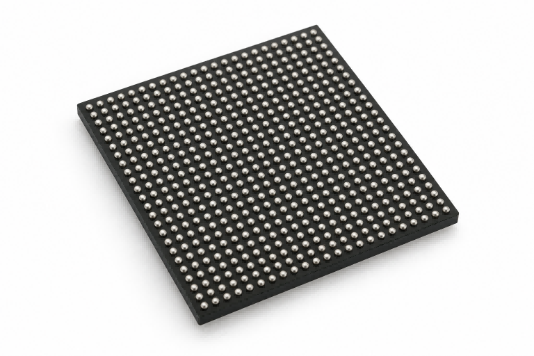
FFG676 is a 27 × 27 mm, 1.0 mm-pitch package with 676 balls, of which up to 400 are available as user I/O on XC7K160T. Power, ground, configuration, GTX, analog, and other dedicated functions use the remaining positions.
Check the schematic and footprint against the official XC7K160T FFG676 pinout. It identifies the 250 HR I/O, 150 HP I/O, GTX lanes, reference clocks, configuration pins, and dedicated power positions. A generic 676-ball package drawing shows the outline but not these device-specific assignments.
The package suffix must match the released footprint and pin map. A mechanically similar Kintex-7 package may expose different I/O or transceiver resources and cannot be selected from outline dimensions alone.
Can You Replace XC7K160T-2FFG676C with Another Part?
A replacement is acceptable only when AMD documents the exact transition or the candidate has been checked against the existing design. A related Kintex-7 part or another device with the same ball count is not automatically pin-compatible.
Changing the package can alter the footprint, ball map, available I/O, and GTX capability. A different speed grade changes timing limits, while a different temperature grade changes the qualified junction range. Moving to another density can also affect logic, memory, DSP, clocking, and transceiver resources.
AMD lists XC7K160T-2FFG676C as the replacement for XC7K160T-2FFV676C. Any other candidate remains a separate engineering proposal until its full order code and documented differences are acceptable for the current board and design.
What Should You Check Before Buying XC7K160T-2FFG676C?
A usable quotation should identify the exact part, material condition, confirmed quantity, delivery basis, included lots, and supporting evidence. These details show whether two offers describe the same purchase rather than superficially similar stock.
- Exact part and condition: The quote should state XC7K160T-2FFG676C and identify whether the material is factory-sealed, opened, repacked, or otherwise nonstandard.
- Confirmed quantity: Separate units physically available for the order from quantities that still depend on sourcing, transfer, or inspection.
- Delivery basis: Request an expected ship date or lead time tied to the confirmed quantity instead of relying on a generic catalog estimate.
- Date code and lot code: Set the acceptable date-code range and state whether the order requires one lot or permits mixed lots.
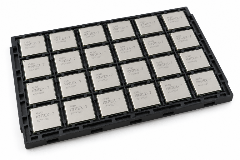
- Packaging: Confirm the tray type, moisture-barrier packaging, label condition, seal status, humidity indication, desiccant, and any repacking.
- Inspection evidence: Define the required photographs, inspection method, sample quantity, and exact lot covered by each report.
Compare offers using the same OPN, condition, quantity, delivery basis, lot rules, packaging, and inspection scope. A lower price is not directly comparable if the underlying offer is different.
Why Source XC7K160T-2FFG676C from Melson Components?
Melson combines controlled sourcing with in-house inspection, retained records, and BOM/EOL support. For XC7K160T-2FFG676C, this gives buyers more information about where the offered material comes from and what checks can support the order.
- Controlled AVL supplier network: Melson works through qualified supply channels and retains sourcing records, reducing dependence on material with an unknown origin.
- In-house inspection support: Available checks include visual inspection, X-ray, decapsulation, LCR, and functional testing when required, allowing the inspection scope to reflect the source and order risk.
- 15-year traceability records: RFQ, sourcing, inspection, packing, and shipment records can be retained for later quality review.
- BOM and EOL support: Melson can review availability and EOL risk, then document alternative options separately for engineering evaluation.
The practical benefit is a quotation connected to the offered source, agreed inspection plan, and retained order records. Buyers can review what is confirmed before placing the order instead of relying on an unqualified stock listing.
What Information Is Required for an XC7K160T-2FFG676C Quote?
Include every requirement that can change availability, delivery, packaging, or inspection. A complete RFQ lets the supplier quote the intended order without filling in important conditions by assumption.
- Part and quantity: XC7K160T-2FFG676C and the required unit count
- Delivery: Target delivery date and ship-to country or location
- Lot requirements: Acceptable date-code range and single-lot or mixed-lot rule
- Condition and packaging: Factory-seal, tray, moisture-barrier, and repacking requirements
- Inspection: Required photographs, tests, reports, and sample quantity
- Substitution: Whether alternatives may be proposed for separate review
Providing these details at the start reduces follow-up and makes quotations easier to compare. Lot, packaging, or inspection requirements added later may change the quoted material.
FAQs About XC7K160T-2FFG676C
Q1: Does XC7K160T include a hard ARM processor?
A1: No. It is an FPGA without the hard processing system used in Zynq-7000 devices. A soft processor can be implemented in programmable logic if the design needs one.
Q2: Does XC7K160T-2FFG676C retain its configuration when power is removed?
A2: No. The FPGA is volatile and must load its configuration at startup from external nonvolatile memory, an external controller, or JTAG.
Q3: What is the minimum configuration-flash size for XC7K160T?
A3: AMD specifies a minimum 64 Mb configuration flash for the 53,540,576-bit full configuration. Multiple images, fallback images, or other stored data may require a larger memory device.
Q4: Which development tool supports XC7K160T-2FFG676C?
A4: AMD Vivado supports the device. Select the exact part identifier xc7k160tffg676-2 so the project uses the correct resources, pinout, and -2 timing model.
Q5: Does XC7K160T include an analog-to-digital converter?
A5: Yes. XC7K160T includes one XADC block. Using it requires the documented analog inputs, references, and board connections.
Q6: Does AMD’s 2040 support statement guarantee stock of this exact part?
A6: No. AMD states support for the 7 Series family through 2040. Availability, quantity, date code, and lead time for this exact part still require a current quotation.
Conclusion
Choose XC7K160T-2FFG676C when the design needs its combination of DSP capacity, block RAM, programmable logic, high-speed serial links, and up to 400 user I/O. Confirm the exact pinout, resource fit, speed grade, and temperature range before releasing the BOM.
For a quotation, send the required quantity, delivery target, date-code and lot rules, packaging condition, and inspection request to sales@melsonchip.com. Melson Components can then check availability and return an offer that reflects the requested purchasing conditions.