 English
 中文
 english


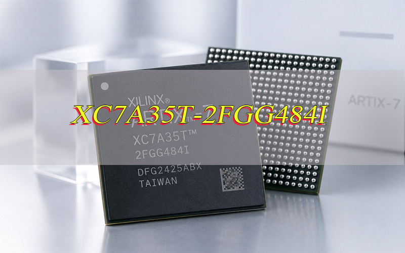
XC7A35T-2FGG484I is an industrial-temperature Artix-7 FPGA designed for applications that require programmable logic, DSP resources, high-speed serial communication, and PCIe connectivity. It combines 33,280 logic cells, 90 DSP48E1 slices, 1,800 Kb of Block RAM, four GTP transceivers, and an FGG484 package, making it suitable for data acquisition, embedded control, and high-speed data transfer.
Before using or sourcing this device, several details matter: the meaning of the full part number, available FPGA resources, PCIe Gen2 support, FGG484 pinout, board-level requirements, temperature grade, and sourcing verification. These factors directly affect device compatibility, system performance, and procurement risk.
What Is XC7A35T-2FGG484I?
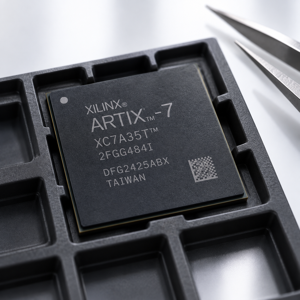
XC7A35T-2FGG484I belongs to the Artix-7 FPGA family. The full ordering code identifies the FPGA device, speed grade, package, and temperature grade.
- XC7A35T: Artix-7 FPGA with 33,280 logic cells.
- -2: Speed grade.
- FGG484: 484-ball BGA package.
- I: Industrial temperature grade.
The I-grade device has a junction temperature range of -40°C to +100°C. For an existing design, the complete part number should be checked because the package, speed grade, and temperature grade can affect compatibility.
XC7A35T-2FGG484I Datasheet Overview
XC7A35T-2FGG484I combines programmable logic, embedded memory, DSP resources, high-speed transceivers, and user I/O. Here is a table and download link of XC7A35T-2FGG484I specifications:
| Specification | XC7A35T-2FGG484I |
|---|---|
| FPGA family | Artix-7 |
| Logic cells | 33,280 |
| CLB slices | 5,200 |
| Maximum distributed RAM | 400 Kb |
| Block RAM | 1,800 Kb |
| DSP48E1 slices | 90 |
| GTP transceivers | 4 |
| Maximum GTP data rate | 6.6 Gb/s |
| Maximum user I/O | 250 |
| Integrated PCIe block | 1 |
| Speed grade | -2 |
| Package | FGG484 |
| Temperature grade | Industrial |
| Junction temperature range | -40°C to +100°C |
What FPGA Resources Does XC7A35T-2FGG484I Provide?
XC7A35T-2FGG484I provides programmable logic, memory, DSP, and serial-transceiver resources within one FPGA.
- 33,280 logic cells: Support state machines, control logic, protocol handling, counters, custom interfaces, and parallel processing.
- 5,200 CLB slices: Provide configurable logic and registers for FPGA functions.
- 1,800 Kb of Block RAM: Suitable for FIFOs, packet buffers, lookup tables, and temporary data storage.
- 400 Kb of distributed RAM: Supports smaller memories implemented within the programmable fabric.
- 90 DSP48E1 slices: Support multiplication, accumulation, filtering, decimation, and other arithmetic operations.
- Four GTP transceivers: Provide serial data rates of up to 6.6 Gb/s per transceiver for supported high-speed interfaces.
Actual resource requirements depend on logic utilization, memory use, DSP demand, clocking, I/O assignments, and timing constraints.
How Does XC7A35T-2FGG484I Support PCIe Gen2?
XC7A35T-2FGG484I supports PCIe Gen2 through four GTP transceivers and an integrated PCI Express block. The FGG484 package supports configurations up to PCIe Gen2 x4.
- PCIe lane width: Supports x1, x2, and x4 configurations.
- GTP transceivers: Four high-speed serial lanes are available for PCIe communication.
- Integrated PCIe block: Handles PCIe protocol functions while programmable logic manages data processing, buffering, and control.
- Reference clock: A low-jitter PCIe reference clock must be connected to the appropriate transceiver clock inputs.
- PCB routing: Differential impedance, pair matching, via transitions, AC coupling, and connector routing must meet PCIe signal-integrity requirements.
- Bandwidth: The selected lane width should match the required data-transfer rate between the FPGA and the host.
For continuous high-volume data transfer, PCIe bandwidth should be calculated together with FPGA processing and buffering requirements.
How Is XC7A35T-2FGG484I Used in High-Speed Data Acquisition?
XC7A35T-2FGG484I can capture, process, buffer, and transfer data between an ADC and a host system.
ADC → FPGA → Digital Processing → Buffer → PCIe/High-Speed Interface → Host
- Data capture: Receives digital output from ADCs through supported parallel, LVDS, or other compatible interfaces.
- Channel alignment: Synchronizes data from multiple channels before processing.
- Signal processing: The 90 DSP48E1 slices support filtering, multiplication, accumulation, decimation, and other real-time calculations.
- Data buffering: 1,800 Kb of Block RAM can be used for FIFOs and short-term data storage.
- Trigger and timing control: Programmable logic can handle event detection, timestamps, acquisition triggers, and timing control.
- Data transfer: Processed or buffered data can be sent to the host through PCIe or another supported high-speed interface.
Device suitability depends on sample rate, channel count, bit depth, processing load, buffer size, and output bandwidth. If the incoming data rate exceeds the sustained host-transfer rate, additional buffering, data reduction, or external memory may be required.
What Should You Know About the XC7A35T-2FGG484I Pinout?
The FGG484 package includes user I/O, power, ground, clock, configuration, analog, and GTP transceiver pins. The 484 package balls are not all available as GPIO.
- User I/O pins: Connect the FPGA to memory, ADCs, control signals, and other digital interfaces.
- I/O bank pins: User I/O is divided into banks, and each bank must use a compatible VCCO voltage and I/O standard.
- Clock-capable pins: Support system clocks and other timing-sensitive signals.
- GTP transceiver pins: Dedicated differential TX and RX pairs support PCIe and other compatible high-speed serial interfaces.
- GTP reference clock pins: Provide the differential reference clocks required by the transceivers.
- Configuration and JTAG pins: Support FPGA programming, configuration, debugging, and device control.
- Power and ground pins: Supply the FPGA core, auxiliary circuits, I/O banks, Block RAM, and transceiver resources.
- XADC and analog pins: Support internal monitoring and external analog measurements.
XC7A35T in the FGG484 package provides up to 250 user I/O pins. Pin assignment should focus on I/O bank voltage, I/O standard, clock location, GTP lane placement, configuration pins, and power connections.
For an existing PCB, use the exact XC7A35T-2FGG484I pinout when checking the schematic and constraint file. Another Artix-7 device using an FGG484 package should not be assumed to be fully pin-compatible.
What Board-Level Requirements Matter for XC7A35T-2FGG484I?
Power, clocking, high-speed routing, configuration, and thermal design directly affect FPGA operation.
- Power rails: Check VCCINT, VCCAUX, VCCBRAM, VCCO, and transceiver supply requirements.
- I/O bank voltages: VCCO must match the I/O standards assigned to each bank.
- Decoupling: Place suitable decoupling capacitors close to the relevant FPGA power pins.
- GTP routing: PCIe and other high-speed differential pairs require controlled impedance, suitable reference planes, correct pair routing, and carefully planned via transitions.
- Clocking: Use the correct clock-capable and GTP reference clock pins for timing-sensitive signals.
- Configuration: Confirm the configuration mode, boot memory, JTAG connections, mode pins, and programming interface before PCB routing.
- Thermal management: Power dissipation depends on resource utilization, switching activity, clock frequency, I/O loading, and transceiver use.
For the industrial-temperature version, the junction temperature must remain within the specified -40°C to +100°C range.
XC7A35T-2FGG484I vs. XC7A35T-2FGG484C: What Is the Difference?
XC7A35T-2FGG484I and XC7A35T-2FGG484C use the same XC7A35T FPGA, -2 speed grade, and FGG484 package. The main difference is the temperature grade.
| Item | XC7A35T-2FGG484I | XC7A35T-2FGG484C |
|---|---|---|
| FPGA family | Artix-7 | Artix-7 |
| Device | XC7A35T | XC7A35T |
| Speed grade | -2 | -2 |
| Package | FGG484 | FGG484 |
| Temperature grade | Industrial | Commercial |
| Junction temperature range | -40°C to +100°C | 0°C to +85°C |
| Suffix | I | C |
The industrial version is specified for a wider temperature range. For an existing BOM, the commercial-temperature version should not automatically replace the industrial version simply because the FPGA device, package, and speed grade are the same.
Why Choose Melson Components for XC7A35T-2FGG484I Sourcing?
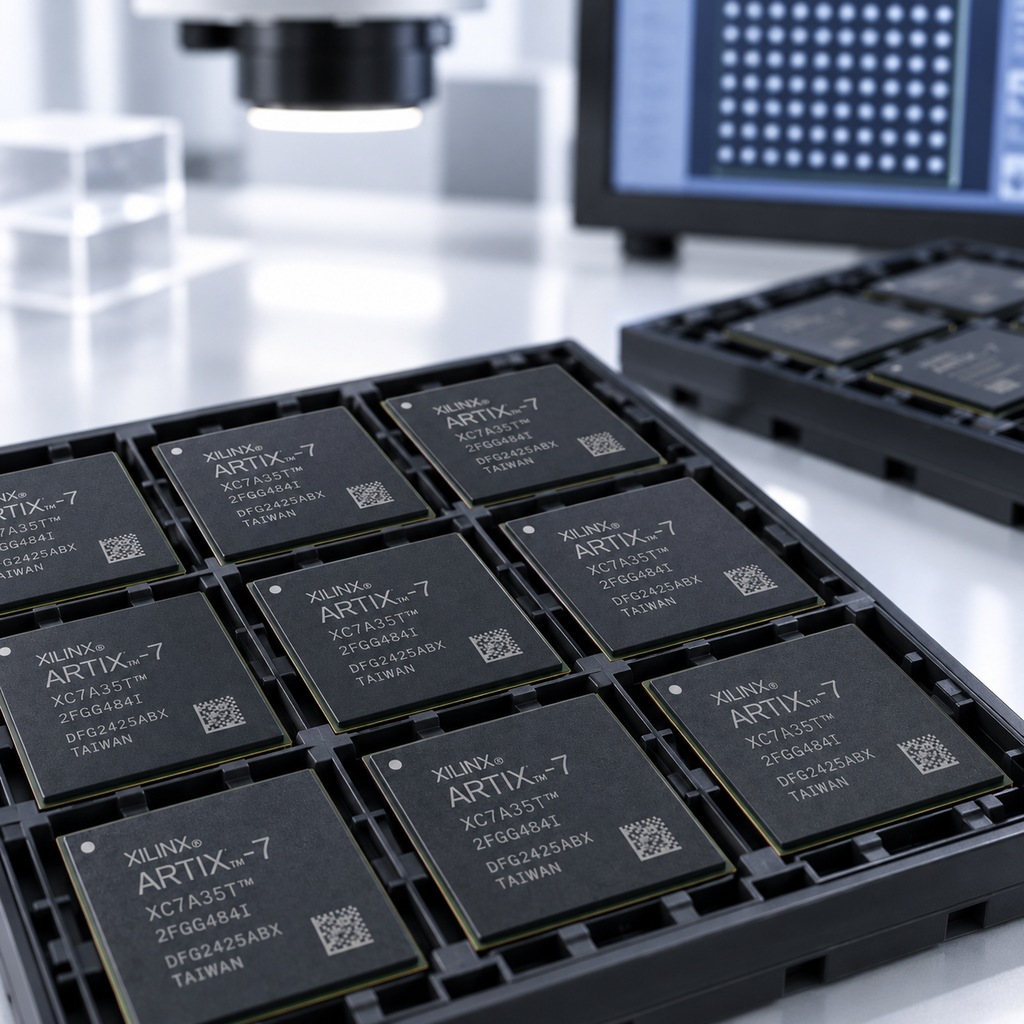
For XC7A35T-2FGG484I, the complete part number, package, speed grade, temperature grade, date code, packaging condition, and available inspection evidence should be checked before shipment.
- Inspection and test support: Visual inspection, X-Ray, De-Cap, and functional testing can be arranged according to component risk and customer requirements.
- Up to 15 years of traceability: RFQ, sourcing, inspection, packing, and shipment records can be retained for up to 15 years.
- Lot-by-lot sourcing verification: Supplier records, label photos, packaging photos, device markings, date codes, and inspection results can be reviewed instead of relying only on online stock quantities.
- Exact-part control: The FGG484 package, -2 speed grade, and industrial temperature grade can be specified as no-substitution requirements.
- Packaging and date-code checks: Outer-box, tray, top-label, packing-list, moisture-barrier bag, seal condition, and date-code information can be requested before shipment.
- Independent sourcing support: Melson is an independent electronic component sourcing partner. Available sourcing and inspection evidence is evaluated for each lot rather than relying on authorized-channel status alone.
Would you like to get a quote for XC7A35T-2FGG484I? Send your quantity, date code requirement, and delivery location to Melson Components via sales@melsonchip.com. Include any specific packaging, inspection, testing, or no-substitution requirements with your RFQ.
FAQs About XC7A35T-2FGG484I
Q1: Is XC7A35T-2FGG484I an Artix-7 FPGA?
A1: Yes. XC7A35T-2FGG484I is an Artix-7 FPGA with 33,280 logic cells, 90 DSP48E1 slices, 1,800 Kb of Block RAM, and four GTP transceivers.
Q2: What does the I suffix mean in XC7A35T-2FGG484I?
A2: The I suffix indicates the industrial temperature grade, with a junction temperature range of -40°C to +100°C.
Q3: Is the -2 speed grade faster than -1?
A3: Yes. The -2 speed grade provides higher timing performance than -1 within the applicable Artix-7 device options.
Q4: Does XC7A35T-2FGG484I support PCIe x4?
A4: Yes. The XC7A35T in the FGG484 package supports PCIe Gen2 configurations up to x4.
Q5: How many GTP transceivers does XC7A35T-2FGG484I have?
A5: It has four GTP transceivers, each supporting data rates of up to 6.6 Gb/s.
Q6: Does the FGG484 package provide 484 user I/O pins?
A6: No. FGG484 refers to the package and ball count. It also includes power, ground, configuration, clock, transceiver, XADC, and other dedicated connections. XC7A35T supports up to 250 user I/O pins.
Q7: Can XC7A35T-2FGG484I be used for high-speed data acquisition?
A7: Yes. Its programmable logic, 90 DSP48E1 slices, 1,800 Kb of Block RAM, and four GTP transceivers support data capture, processing, buffering, and high-speed transfer. The required sample rate, channel count, bit depth, and bandwidth must still fit within the available resources.
Q8: Can XC7A35T-2FGG484I connect to DDR3 memory?
A8: Yes. External DDR3 memory can be used when the selected I/O banks, controller configuration, voltage, timing, and PCB routing meet the interface requirements.
Q9: Are all Artix-7 FGG484 devices directly interchangeable?
A9: No. Check the device-specific pinout, I/O banks, GTP locations, power connections, FPGA resources, speed grade, and temperature grade before considering a substitution.
Q10: Can an online stock quantity confirm that all XC7A35T-2FGG484I parts come from the same lot?
A10: No. Website stock quantity does not confirm lot or date-code consistency. Quotation details, labels, packaging, physical markings, and supporting records should be checked when a consistent lot is required.
Q11: What should be checked when buying older XC7A35T-2FGG484I stock?
A11: Check the complete ordering code, date code, lot information, device markings, tray or moisture-barrier packaging, label information, packaging condition, sourcing records, and required inspection results.
Q12: What information is needed for an XC7A35T-2FGG484I RFQ?
A12: Send the quantity, date code requirement, and delivery location. Add any specific no-substitution, packaging, inspection, testing, or documentation requirements.