 English
 中文
 english

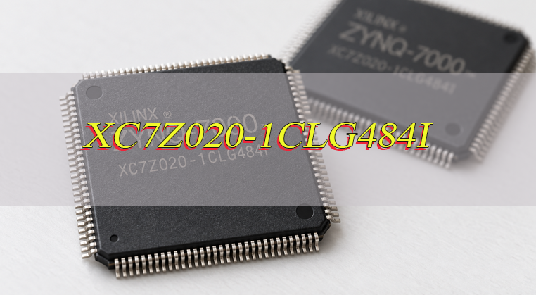
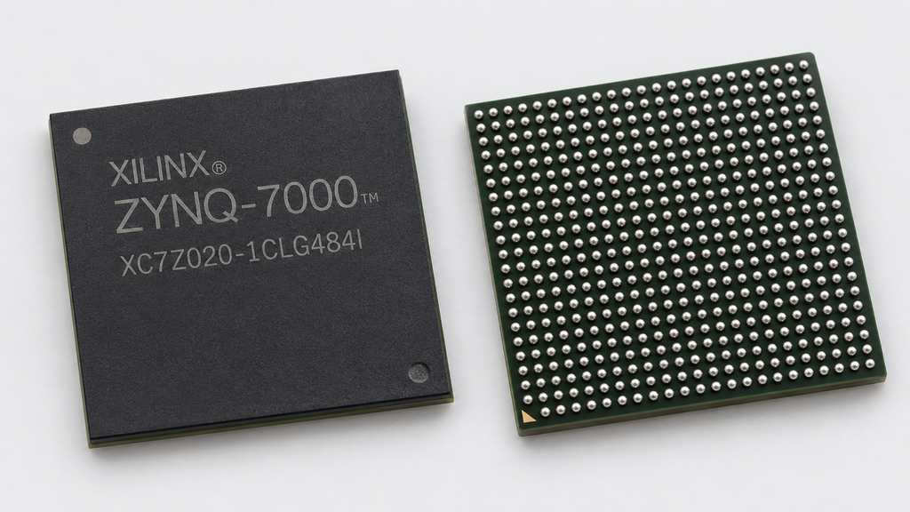
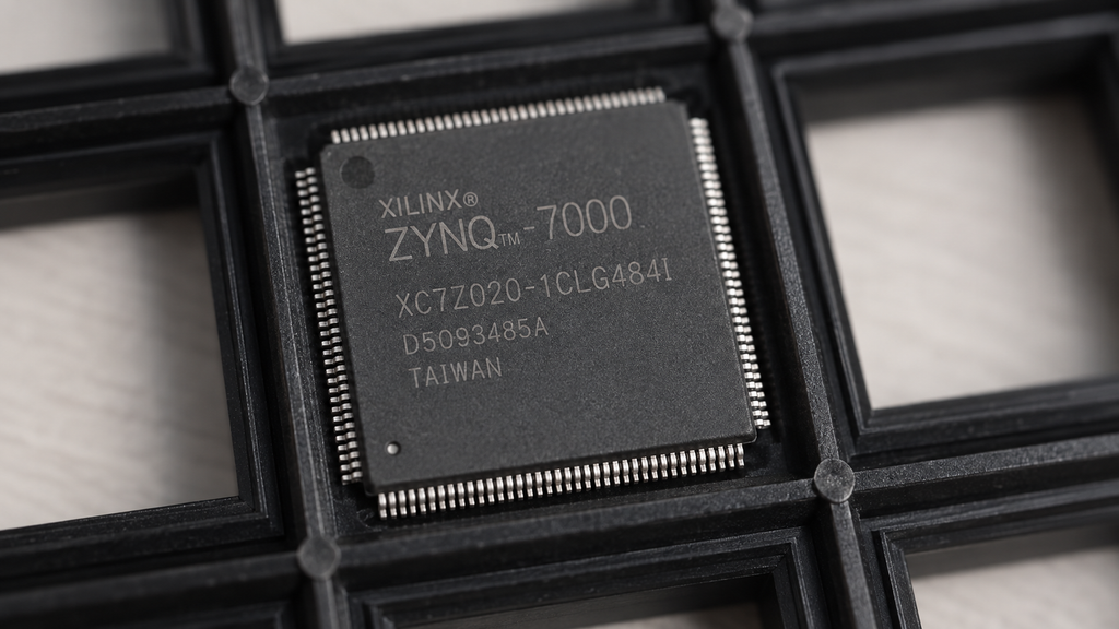
XC7Z020-1CLG484I is an XC7Z020 Zynq-7000 SoC in the 484-ball CLG package, with -1 speed grade and industrial temperature qualification. For pin assignment, the XC7Z020 device and CLG484 package determine the ball map; the speed and temperature suffixes still matter for timing and electrical qualification, but they do not create another CLG484 coordinate table. A safe design therefore starts with the exact package file, then checks processing-system MIO and DDR separately from programmable-logic I/O.
The practical path is AMD package CSV to Vivado part selection to PS configuration and XDC to schematic symbol to BGA footprint. Following that order prevents a generic XC7Z020 diagram, a different package, or a third-party CAD symbol from replacing the authoritative XC7Z020-1CLG484I package record.
Which AMD Datasheet and Pinout Files Apply to XC7Z020-1CLG484I?
The exact ball-level sources are xc7z020clg484pkg.csv and xc7z020clg484pkg.txt from AMD’s Zynq-7000 package-pinout ZIP. Use UG865 to interpret those files, UG585 to configure PS MIO and boot behavior, DS187 for electrical and timing limits, and UG933 for board-level DDR and power implementation. No single AMD document covers every pin-assignment decision.
- Exact package mapping: Download the current Zynq-7000 ZIP from AMD’s package device pinout files page and select xc7z020clg484pkg.csv or the equivalent text file. These files map every CLG484 coordinate to its pin name, bank and I/O type.
- Package-file interpretation: UG865, Zynq-7000 SoC Packaging and Pinout, defines the CLG484 package, the top-view ball diagrams and the package-file columns. It is the check for orientation, package dimensions and naming conventions.
- Processing-system assignment: UG585, Zynq-7000 SoC Technical Reference Manual, controls MIO peripheral routing, EMIO use, boot straps and reset behavior. The package CSV supplies coordinates; UG585 supplies PS behavior.
- Device limits: DS190 identifies XC7Z020 resources, while DS187 supplies DC, AC and speed-grade limits. Use the -1 and industrial-grade limits that match the ordered device rather than carrying limits from another Zynq part.
- PCB implementation: UG933 covers power distribution, decoupling, DDR reference requirements and layout checks. It does not replace the exact CLG484 pin list.
Keep the downloaded package-file revision with the schematic release. If AMD updates the file or the design changes package, compare the new file against the released pin-assignment record before reusing the symbol or footprint.
How Is the XC7Z020-1CLG484I Pinout Organized?
The XC7Z020-1CLG484I pinout is divided into PS MIO, fixed PS DDR, four PL SelectIO banks, configuration/JTAG pins, analog pins, power and ground. Filter the 484 coordinate records by function and bank before checking individual balls; a flat alphabetical scan hides shared voltage and routing constraints.
- PS MIO: MIO0 through MIO53 provide 54 multiplexed processing-system pins. UG585 calls MIO0-15 MIO Bank 0 and MIO16-53 MIO Bank 1; the package CSV identifies these physical domains as banks 500 and 501.
- PS DDR: Bank 502 contains the dedicated DDR data, strobes, masks, address, command, clock, reference and calibration signals. These pins are not interchangeable with PL I/O.
- PL SelectIO: Banks 13, 33, 34 and 35 each contain 50 HR I/O pins, for 200 programmable-logic I/O pins in CLG484.
- Configuration bank: Bank 0 contains dedicated configuration and JTAG signals such as PROGRAM_B, INIT_B, DONE, CFGBVS, TCK, TMS, TDI and TDO. It is not the same domain as PS MIO Bank 0.
- Non-user I/O: The remaining balls include power, ground, XADC-related pins, references, reserved connections and other dedicated functions. A ball that is not ordinary user I/O still needs an intentional schematic connection or an explicit no-connect decision from the official documentation.
The CSV reports 58 entries with I/O type MIO, not 58 numbered MIO pins. That total includes the 54 MIO signals plus PS_CLK, PS_POR_B, PS_SRST_B and PS_MIO_VREF. Separating the classification count from the numbered MIO count prevents four special PS pins from being mistaken for extra peripheral routes. If a symbol reports 58 numbered MIO signals or merges bank 0 with bank 500, record it as a pin-classification error and correct it before net assignment.
How Do You Read the CLG484 Ball Map?
Read each CLG484 location as a top-view BGA coordinate, then decode its pin name and bank before assigning a function. CLG484 is a 0.80 mm-pitch package with 22 lettered rows and columns 1 through 22. The row sequence is A, B, C, D, E, F, G, H, J, K, L, M, N, P, R, T, U, V, W, Y, AA and AB, so ambiguous letters are intentionally skipped.
- Locate the coordinate: A name such as F7 identifies one physical package ball. Confirm the A1 orientation mark on the package drawing and footprint; do not mirror a top-view map into the PCB land pattern by eye.
- Read the full pin name: IO_L11N_SRCC_13, for example, identifies a PL I/O in bank 13, the N side of differential pair L11, with regional clock capability. The coordinate and the complete name together form the useful identity.
- Check the Bank column: Bank membership determines the voltage domain and available resources. Similar-looking names in different banks are not electrically interchangeable.
- Check I/O Type and special columns: The CSV distinguishes HR, MIO, DDR, CONFIG and non-general-I/O records. Memory-byte-group and VCCAUX-group fields add routing or power context where applicable.
- Honor reserved and no-connect status: A migration or reserved note is a connection rule, not spare routing capacity. Preserve the official disposition in the schematic and footprint review.
A screenshot of the CLG484 ball map is useful for orientation, but the CSV supports a stronger net-by-net check because it can be sorted, filtered and compared with an exported pin list. Use the diagram to understand placement and the machine-readable file to verify identity. This comparison exposes a mirrored footprint, a skipped row or a copied pin-name error before PCB release.
How Are the MIO Pins Assigned on XC7Z020-1CLG484I?
MIO0-15 are in package bank 500 and MIO16-53 are in package bank 501; their peripheral functions are selected in the Zynq Processing System configuration, not remapped with ordinary PL XDC constraints. If a PS peripheral cannot use the chosen MIO route, EMIO carries that peripheral through the programmable logic and then to a PL I/O pin.
- MIO0-15, bank 500: 0 G6, 1 A1, 2 A2, 3 F6, 4 E4, 5 A3, 6 A4, 7 D5, 8 E5, 9 C4, 10 G7, 11 B4, 12 C5, 13 A6, 14 B6, 15 E6.
- MIO16-31, bank 501: 16 D6, 17 E9, 18 A7, 19 E10, 20 A8, 21 F11, 22 A14, 23 E11, 24 B7, 25 F12, 26 A13, 27 D7, 28 A12, 29 E8, 30 A11, 31 F9.
- MIO32-47, bank 501: 32 C7, 33 G13, 34 B12, 35 F14, 36 A9, 37 B14, 38 F13, 39 C13, 40 E14, 41 C8, 42 D8, 43 B11, 44 E13, 45 B9, 46 D12, 47 B10.
- MIO48-53, bank 501: 48 D11, 49 C14, 50 D13, 51 C10, 52 D10, 53 C12.
The two MIO banks have separate supply domains: VCCO_MIO0 is on B3 and C6, while VCCO_MIO1 is on A10, B13, D9 and E12. Select each bank voltage from the peripherals and standards assigned to that bank. Also reserve PS_CLK at F7, PS_POR_B at B5, PS_SRST_B at C9 and PS_MIO_VREF at F8 before treating nearby coordinates as ordinary MIO.
MIO7 and MIO8 are output-only during normal MIO operation, and MIO2 through MIO8 also participate in boot-mode sampling. That dual role makes boot-strapping, bank voltage and peripheral assignment one combined schematic check rather than three independent decisions. Verify the configured peripheral route and the sampled strap state together; a mismatch can select the wrong boot mode even when the post-boot signal name looks correct.
How Are the DDR Pins Grouped in the CLG484 Package?
The CLG484 PS DDR interface is a fixed 32-bit bus in bank 502, arranged as four byte lanes with eight DQ pins, one DM pin and one differential DQS pair per lane. Keep each lane and its strobe together during schematic review and PCB planning; these signals are not freely swappable with MIO or PL pins.
| Byte Lane | DQ Ball Order | DM Ball | DQS P/N |
|---|---|---|---|
| DQ0-7 | D1, C3, B2, D3, E3, E1, F2, F1 | B1 | C2 / D2 |
| DQ8-15 | G2, G1, L1, L2, L3, K1, J1, K3 | H3 | H2 / J2 |
| DQ16-23 | M1, T3, N3, T1, R3, T2, M2, R1 | P1 | N2 / P2 |
| DQ24-31 | AA3, U1, AA1, U2, W1, Y3, W3, Y1 | AA2 | V2 / W2 |
The address pins A0-A14 map in order to M4, M5, K4, L4, K6, K5, J7, J6, J5, H5, J3, G5, H4, F4 and G4. BA0-BA2 are L7, L6 and M6. The main control group includes CAS_B at P3, CKE at V3, CK_P/CK_N at N4/N5, CS_B at P6, DRST_B at F3, ODT at P5, RAS_B at R5 and WE_B at R4.
Reference and calibration pins are part of the same interface: DDR_VREF0 is H7, DDR_VREF1 is P7, DDR_VRP is N7 and DDR_VRN is M7. The nine VCCO_DDR balls are E2, F5, H1, J4, K7, M3, N6, R2 and V1. Configure this fixed PS DDR interface in the Zynq Processing System block rather than treating it as a PL Memory Interface Generator pin set. Verify the memory topology, width, reference network, drive settings and trace-delay targets against the current UG585 and UG933 guidance. A cross-lane DQ/DQS mismatch or omitted package delay can invalidate timing even when the PCB copper lengths appear matched.
How Are the PL I/O Banks Organized on XC7Z020-1CLG484I?
XC7Z020-1CLG484I exposes four HR programmable-logic banks: 13, 33, 34 and 35, each with 50 I/O pins. Every bank contains 24 true differential P/N pairs plus two additional single-ended I/O pins, so the CLG484 package provides 200 PL I/O pins without implying 100 freely interchangeable differential interfaces.
| PL Bank | HR I/O | Differential Resources | VCCO Balls |
|---|---|---|---|
| 13 | 50 | 24 P/N pairs plus 2 single-ended pins | 7 |
| 33 | 50 | 24 P/N pairs plus 2 single-ended pins | 6 |
| 34 | 50 | 24 P/N pairs plus 2 single-ended pins | 6 |
| 35 | 50 | 24 P/N pairs plus 2 single-ended pins | 7 |
Assign a PL port with the exact PACKAGE_PIN coordinate and its IOSTANDARD in the XDC. The bank number identifies a shared electrical domain, not a signal voltage: all interfaces placed in one bank must be compatible with that bank’s VCCO and any required reference voltage. The package CSV places VCCO_13 at AA10, AB3, T5, U8, V11, W4 and Y7; VCCO_33 at AA20, AB13, U18, V21, W14 and Y17; VCCO_34 at K17, L20, N16, P19, R22 and T15; and VCCO_35 at A20, C16, D19, E22, F15, G18 and H21. Vivado DRC should confirm bank-voltage, I/O-standard, differential-pair and clock-routing compatibility before the schematic is released.
The two unpaired pins in each bank are named IO_0 and IO_25. Treat them as single-ended resources. Counting every 50-pin bank as 25 differential pairs would create four nonexistent mates and can propagate directly into an incorrect symbol or routing plan.
How Are Differential Pairs and Clock-Capable I/O Pins Identified in CLG484?
A differential pair shares the same IO_L number and bank suffix, with P and N identifying the two mates; MRCC or SRCC in the name marks clock-capable resources. Each CLG484 PL bank has two MRCC pairs and two SRCC pairs. Use both the coordinate and the full name when constraining a clock or high-speed pair.
| Bank | MRCC P/N Balls | SRCC P/N Balls |
|---|---|---|
| 13 | Y9/Y8; Y6/Y5 | AA9/AA8; AA7/AA6 |
| 33 | Y18/AA18; W17/W18 | Y19/AA19; W16/Y16 |
| 34 | L18/L19; M19/M20 | K19/K20; N19/N20 |
| 35 | D18/C19; B19/B20 | C17/C18; D20/C20 |
In a name such as IO_L14P_T2_AD4P_SRCC_35, L14P identifies the P side of pair 14, T2 identifies its byte-group position, AD4P identifies an auxiliary analog-capable role, SRCC identifies single-region clock capability and _35 identifies bank 35. These fields describe different resources; none should be dropped from the review record.
For a single-ended clock input on a differential clock-capable pair, use the P side as required by the 7-series clocking guidance. Clock-capable marking makes the ball eligible for clock routing, but the chosen buffer, region reach, I/O standard and placement still need Vivado validation. A P/N name also does not authorize polarity swapping unless the selected interface, primitive and implementation flow explicitly support it.
Which Power, Ground, Reset, JTAG, and Boot Pins Need Special Attention?
Protect the dedicated PS clock/reset, boot straps, JTAG/configuration pins, analog references, reserved balls and every supply domain before assigning ordinary signals. Treating a dedicated or shared-function ball as spare I/O, or powering a bank for an incompatible interface standard, creates a direct schematic error before routing begins.
- PS clock and reset: PS_CLK is F7, PS_POR_B is B5 and PS_SRST_B is C9. Meet the clock and reset timing requirements, and hold power-on reset until the required rails and clock are valid.
- Boot straps: MIO2 A2, MIO3 F6, MIO4 E4, MIO5 A3, MIO6 A4, MIO7 D5 and MIO8 E5 are sampled at boot. Set the required pull direction and confirm that the selected boot peripheral does not conflict with the strap state or bank voltage.
- Dedicated JTAG: TCK is G11, TMS is G12, TDI is H13 and TDO is G14. Preserve the intended chain and debug access; do not assign these bank-0 balls as PL user I/O.
- PL configuration: PROGRAM_B is T11, DONE is T12, CFGBVS is T13, INIT_B is T14 and PUDC_B is K16. Match CFGBVS to VCCO_0 and implement PUDC_B and configuration-mode behavior for the board’s power-up strategy.
- XADC and references: VP is L11, VN is M12, VREFP is M11, VREFN is L12, VCCADC is K11 and GNDADC is K12. Follow the analog-supply and unused-input guidance; do not route these as ordinary digital I/O.
- Reserved connections: RSVDGND is G10, RSVDVCC1 is T7, RSVDVCC2 is T8 and RSVDVCC3 is T10. Connect them exactly as the current AMD package and configuration guidance requires.
The package also contains separate VCCINT, VCCAUX, VCCBRAM, VCCPINT, VCCPAUX, VCCPLL, VCCO_0, VCCO_MIO0, VCCO_MIO1, VCCO_DDR and PL-bank VCCO domains, plus 63 ground balls. Use the exact CSV power-pin inventory and the current power-sequencing requirements. Connecting all pins labeled VCC to one rail is not a valid simplification.
UG585 specifies that MIO2 through MIO8 are sampled after PS_POR_B is deasserted. MIO2-6 select boot and related options, while MIO7-8 set MIO bank voltage mode. Review the boot resistors together with the connected peripheral and its powered state so an external device cannot force an unintended strap level at reset release.
What Should You Verify When Matching XC7Z020-1CLG484I to Your Design Requirements?
Release the design only when the same XC7Z020 and CLG484 identity agrees across AMD’s package file, Vivado, PS configuration, XDC, schematic and footprint. The check must prove both directions: every used design signal reaches the intended ball, and every dedicated or powered ball has the required connection.
- Select the exact Vivado part. Choose xc7z020clg484-1 and record the tool/device-file version. The project part must show XC7Z020, CLG484 and -1 rather than CLG400 or another Zynq device/package.
- Freeze the package source. Keep xc7z020clg484pkg.csv with its download date and hash in the design record. This becomes the reproducible coordinate-to-pin baseline for every symbol and footprint comparison.
- Export the PS configuration. Review MIO peripheral routing, EMIO choices, VCCO_MIO0/VCCO_MIO1, boot mode, PS_CLK and reset settings. The exported configuration must agree with the schematic nets, strap components and powered I/O domains.
- Constrain every PL port. Give each top-level PL port an exact PACKAGE_PIN and compatible IOSTANDARD, then run Vivado I/O and DRC reports. Release only with zero unconstrained ports and no unresolved bank-voltage, differential-pair or clock-resource conflict.
- Audit the DDR interface by group. Compare every DQ byte lane, DM, DQS pair, address, command, clock, VREF, VRP/VRN and VCCO_DDR net with the package file and memory configuration. The resulting DDR netlist should contain no cross-lane or P/N transcription error.
- Compare the schematic symbol pin by pin. Sort or script-compare symbol pin numbers and names against the AMD CSV. Record every difference; only documented aliases or intentional no-connects may remain.
- Verify the footprint from A1 outward. Check the top/bottom-view convention, row letters, columns, 0.80 mm pitch, body outline and ball count against UG865. A footprint overlay or coordinate report should show 484 unique pads with no mirror error or duplicate coordinate.
- Close power, reset and boot dependencies. Review each rail, reference, ground, reserved ball, strap resistor and power-on state as one startup path. The review must demonstrate the intended boot mode without exposing an I/O bank to an incompatible supply.
- Run a final netlist-to-pin comparison. Compare the implemented Vivado pin report, approved schematic netlist and footprint pad list before PCB layout release. The controlled mismatch report must close at zero unexplained items.
A pin-compatible sourcing decision also needs the full orderable identity. If the package, speed grade or temperature suffix differs from XC7Z020-1CLG484I, stop the release and repeat the applicable timing, qualification and package checks rather than assuming the new device is a drop-in replacement.
FAQs About the XC7Z020-1CLG484I Pinout
Q1: Are XC7Z020-1CLG484I and XC7Z020-1CLG484C pin-compatible?
A1: The physical CLG484 ball coordinates are the same when the device and package remain XC7Z020 and CLG484. The two orderable parts are not qualification-equivalent because the I and C suffixes select different temperature grades. Recheck the applicable electrical, timing and operating-temperature limits before approving the commercial-grade part for an industrial design.
Q2: Can EMIO use an unused MIO ball?
A2: No. EMIO does not convert an unused MIO coordinate into a programmable-logic pin. It routes a processing-system peripheral through the PL fabric, after which the signal must reach an available PL I/O ball with a valid PACKAGE_PIN, IOSTANDARD and bank-voltage assignment. Confirm the complete route in the PS configuration and Vivado implementation.
Q3: Are PS MIO Bank 0 and configuration Bank 0 the same bank?
A3: No; they are separate pin domains. UG585 uses MIO Bank 0 for MIO0-15, while the CLG484 package file identifies that physical MIO supply domain as bank 500. Package bank 0 contains dedicated configuration and JTAG functions. Keeping these names separate prevents the wrong supply or signal rules from being applied.
Q4: Is a PACKAGE_PIN constraint enough for a PL signal?
A4: No. PACKAGE_PIN identifies the ball but does not complete the electrical constraint. Assign the compatible IOSTANDARD, confirm the bank VCCO and any reference-voltage requirement, and check differential-pair or clock-capable routing where applicable. Vivado I/O and DRC reports should close without unconstrained ports or bank-resource conflicts.
Q5: Can DDR DQ bits be swapped within a byte lane?
A5: Only use a bit swap that the current Zynq PS DDR configuration flow and selected memory interface explicitly support. The package map alone does not approve a change. Preserve each byte lane, DM and DQS association, then verify any permitted DQ swap in the generated configuration, schematic, routed netlist and timing analysis.
Q6: Can pin assignments from another XC7Z020 package be copied into CLG484?
A6: No. Device-family identity does not make different packages ball-compatible. CLG400, CLG484 and other XC7Z020 packages have different coordinate maps and physical footprints. Rebuild or verify the symbol, XDC assignments and land pattern against xc7z020clg484pkg.csv and the CLG484 package drawing before releasing the board.
If you are sourcing XC7Z020-1CLG484I for a new build, production run, maintenance, or replacement requirement, Melson Components can help check availability and sourcing options.
To request a quote, send sales@melsonchip.com your quantity, date code requirement, and delivery location. We will review the requirement based on the exact part number XC7Z020-1CLG484I and reply with the available sourcing options.