 English
 中文
 english


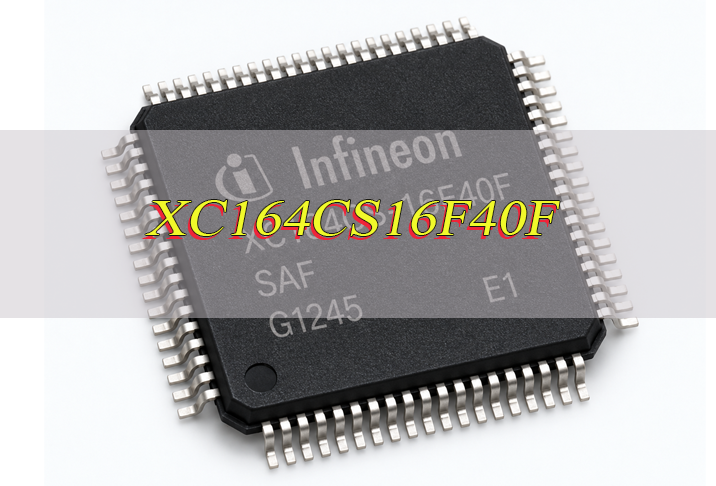
XC164CS16F40F refers to Infineon’s XC164CS-16F40F, a 16-bit MCU with a 40 MHz C166SV2 core, 128 KB Flash, 8 KB RAM, TwinCAN, and a 100-pin TQFP package. The shortened name does not specify the SAK or SAF temperature grade, silicon step, package code, or delivery form, so these details must be confirmed before maintenance, purchasing, or replacement.
The sections below connect those headline specifications to the decisions that matter on a working board: execution timing, memory placement, CAN configuration, pin multiplexing, power sequencing, interrupt latency, and replacement qualification. Together, they show what the XC164CS16F40F can do, which limits must be preserved, and what evidence is needed before an existing design is changed.
What Is the XC164CS16F40F?
The XC164CS16F40F is a deterministic embedded-control MCU in Infineon’s XC166 family. It combines the C166SV2 CPU with on-chip program memory, data RAM, analog inputs, timers, serial interfaces, two CAN controller nodes, and JTAG-based debugging.
Its main use is controlling equipment that must sample inputs, execute time-critical logic, drive outputs, and exchange CAN messages. The MCU is not a complete system: CAN communication still requires external transceivers, and the board must provide the required core and I/O supply rails.
What Does the XC164CS-16F40F Part Number Mean?
XC164CS identifies the device group, 16F identifies the 128 KB Flash derivative, and 40F identifies the 40 MHz speed class. The remaining ordering details appear outside this shortened derivative name.
- XC164CS: XC164CS derivative within the XC166 microcontroller family.
- 16F: 128 KB on-chip Flash. An 8F derivative has 64 KB Flash, while an R derivative uses mask-programmed ROM.
- 40F: Maximum CPU clock of 40 MHz. The corresponding 20F speed class is limited to 20 MHz.
- SAK or SAF: SAK covers -40°C to +125°C ambient operation; SAF covers -40°C to +85°C.
- Step and package suffixes: The complete order code identifies the silicon step, package, and delivery form.
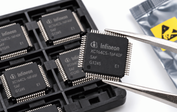
Use XC164CS16F40F for searching and cross-referencing, but use the complete top marking and approved BOM number to accept a device.
What Are the Specifications of the XC164CS16F40F?
The XC164CS-16F40F provides a 40 MHz C166SV2 CPU, 128 KB Flash, 8 KB RAM, two CAN nodes, and a 100-pin TQFP interface. Below is the specifications table and download link for the XC164CS16F40F for your reference:
| Item | Specification |
|---|---|
| CPU | 16-bit C166SV2, five-stage execution pipeline |
| Maximum CPU clock | 40 MHz |
| Typical one-cycle time | 25 ns at 40 MHz |
| Program memory | 128 KB on-chip Flash |
| On-chip RAM | 2 KB DPRAM, 4 KB DSRAM, 2 KB PSRAM |
| Address space | 16 MB linear code and data space |
| CAN | TwinCAN, two nodes, 32 message objects, CAN 2.0B active, up to 1 Mbit/s |
| ADC | 14 channels, programmable 8-bit or 10-bit conversion |
| Timing resources | Two 16-channel CAPCOM units, CAPCOM6, five GPT12E timers, RTC |
| Serial interfaces | Two ASC channels and two SSC channels |
| Interrupt system | 16 priority levels, up to 75 sources, eight PEC channels |
| General-purpose I/O | Up to 79 lines |
| External memory | Up to approximately 12 MB of external RAM or ROM |
| Debug support | JTAG-based OCDS and on-chip bootstrap loader |
| Core supply | 2.35 V to 2.7 V |
| I/O supply | 4.4 V to 5.5 V |
| Package | 100-pin TQFP, 0.5 mm pitch |
| Temperature grades | SAK: -40°C to +125°C; SAF: -40°C to +85°C |
How Is On-Chip Memory Arranged in the XC164CS16F40F?
The XC164CS16F40F uses a unified 16 MB address space, but its 128 KB Flash and three RAM blocks are managed for different types of access. The Program Management Unit handles code fetches from Flash and PSRAM, while the Data Management Unit handles data transfers to DSRAM, DPRAM, and peripherals. Because the two units share the high-speed system bus and can work concurrently, correct placement can reduce contention between instruction fetches and data access.
- 128 KB Flash at C00000H-C1FFFFH: Holds program code and constants. It is organized as four 8 KB sectors, one 32 KB sector, and one 64 KB sector, with 128-byte programming blocks and sector-level protection options.
- 2 KB PSRAM at E00000H-E007FFH: Sits on the program side and is optimized for code fetches. Time-critical routines may be copied here when the linker and startup code are configured for it.
- 4 KB DSRAM: Provides general data storage through the Data Management Unit and is the natural location for frequently accessed runtime data.
- 2 KB DPRAM: Holds variables, the system stack, and global register banks; part of the space is bit-addressable for efficient flag handling.
This arrangement means a firmware image is not portable merely because its total Flash and RAM usage fits. The linker file must preserve section addresses, stack headroom, register-bank allocation, interrupt vectors, protected Flash sectors, and any startup copy from Flash to PSRAM. After a rebuild, compare the link map with the approved version and verify that no section moved across a memory boundary or into an address range used by peripherals or external memory.
How Does TwinCAN Work on the XC164CS16F40F?
TwinCAN places two independent Full-CAN controller nodes around one shared pool of 32 message objects. Each object is assigned to node A or node B and configured for transmit or receive, an 11-bit or 29-bit identifier, an acceptance mask, data length, and interrupt behavior. Objects can also be grouped into FIFOs of 2, 4, 8, 16, or 32 entries when a message stream needs buffering rather than one fixed mailbox.
The two nodes may serve separate CAN networks. In gateway mode, a received object can pass selected data to a transmit object on the other node without making the CPU copy every frame. Up to eight programmable interrupt nodes let firmware separate events such as receive, transmit, error, and gateway traffic by priority. The bit-timing registers derive the CAN time quanta from the master clock and support rates up to 1 Mbit/s, but the configured sample point and baud rate must match the network.
To bring up either node, assign its CAN pins, connect an external physical-layer transceiver, configure bit timing, allocate message objects, set filters, clear pending status, and then enable interrupts or polling. CAN pins can be routed through Port 4 or Port 9; the selected route must match both the PCB nets and the firmware setting. Port 4 sharing also matters when the external bus uses segment-address lines. If no frames are received, check the pin route, transceiver enable state, termination, bus voltage, oscillator accuracy, baud rate, acceptance mask, and message-object ownership in that order.
Which On-Chip Peripherals Are Available on the XC164CS16F40F?
The MCU integrates analog conversion, capture/compare units, timers, serial interfaces, watchdog supervision, external-bus control, GPIO, and debug hardware. Their main functions are:
- ADC: Fourteen multiplexed channels with programmable 8-bit or 10-bit conversion.
- CAPCOM1 and CAPCOM2: Two 16-channel units for event capture, scheduled edges, pulses, and PWM.
- CAPCOM6: Coordinated PWM and capture functions for motor and actuator control.
- GPT12E: Five 16-bit timers for counting, capture, frequency measurement, and incremental interfaces.
- ASC0 and ASC1: UART-style asynchronous communication or synchronous half-duplex operation.
- SSC0 and SSC1: SPI-compatible synchronous master or slave communication.
- RTC and watchdog: Time-base and wake-up functions plus software supervision and reset.
- GPIO, bus, and debug: Up to 79 GPIO lines, an 8-bit or 16-bit external bus, JTAG-based OCDS, and a bootstrap loader.
When checking firmware compatibility, compare register maps, trigger paths, alternate-pin selections, interrupt routing, startup defaults, and timing. Matching peripheral names alone do not prove compatible behavior.
What Power, Clock, and Operating Limits Apply to the XC164CS16F40F?
The MCU requires a 2.35 V to 2.7 V core supply and a separate 4.4 V to 5.5 V I/O supply. Hold RSTIN low until both domains are valid, connect every supply and ground pin, and place decoupling close to the corresponding pin pairs.
- Clock: A crystal or external clock feeds the oscillator; the PLL and prescalers generate the master, CPU, and system clocks. The CPU limit is 40 MHz.
- Flash timing: The Flash uses one wait state at 40 MHz and can use zero wait states at or below 20 MHz under the specified conditions.
- Low-power modes: Idle stops the CPU while selected peripherals run; sleep and power-down stop more of the clock system. Wake-up and watchdog behavior depend on the chosen mode.
- Temperature: SAK devices cover -40°C to +125°C; SAF devices cover -40°C to +85°C.
Validate oscillator startup, PLL settings, reset release, CAN timing, serial baud rates, timer prescalers, and temperature limits under the actual board conditions.
What Should You Know About the XC164CS16F40F Pinout and TQFP-100 Package?
The XC164CS-16F40F uses a 100-pin TQFP with 0.5 mm lead pitch. Because many pins support alternate GPIO, peripheral, bus, debug, clock, reset, or analog functions, package compatibility alone does not guarantee electrical or functional compatibility.
PORT0 and PORT1 mainly support the external bus, while Port 3 combines GPIO, timers, serial interfaces, and bus control. Port 4 and Port 9 can carry CAN functions, Port 5 is mainly used for analog inputs, and Port 20 provides external-bus control signals such as RD, WR, ALE, EA, and RSTOUT.
Check the non-GPIO pins as separate electrical groups:
- Core and I/O supplies: Connect every VDDI/VSSI and VDDP/VSSP pin, keep the 2.5 V core and 5 V pad domains within their specified ranges, and decouple each local pin group.
- Analog references: Route VAREF and VAGND as a quiet reference pair; digital return current or a noisy reference directly affects ADC accuracy.
- Reset and boot control: Hold RSTIN low until both supplies and the clock are valid, verify the documented reset width, and confirm EA and other boot-strap levels at release.
- Oscillator and clock pins: Match the crystal or external-clock network to the clock mode used by the startup code, then verify oscillator startup and PLL lock before normal execution.
- NMI and debug pins: Keep an unused NMI at its required inactive level and prevent TRST/JTAG signals from floating into an unintended debug state.
- CAN and external bus: Confirm whether CAN uses Port 4 or Port 9 and whether that choice conflicts with address, chip-select, or bus-control functions.
For maintenance or replacement, start at pin 1 on the official top-view drawing and compare all 100 pins against the schematic. The finished record should identify each net, configured function, startup level, voltage domain, external component, and unused-pin treatment. Acceptance requires both a net-by-net match and a firmware pin-configuration match; package name and pin count alone are insufficient.
How Does the XC164CS16F40F Handle Interrupts and Time-Critical Tasks?
The interrupt system supports up to 75 sources, 16 priority levels, and a typical eight-clock response for code in internal program memory. Higher-priority services can interrupt lower-priority services, and each standard source has a dedicated vector.
Eight Peripheral Event Controller channels can transfer a byte or word in one CPU cycle without entering a full interrupt routine. Fast external inputs support rising, falling, or dual-edge detection, while hardware traps handle NMI, stack errors, illegal instructions, and access errors.
Worst-case latency must include the current instruction, nested services, PEC traffic, Flash wait states, disabled-interrupt windows, and flag handling. The installed silicon step must also be checked against its matching errata for CPU, interrupt, TwinCAN, Flash, ADC, serial, and timer workarounds.
Where Is the XC164CS16F40F Commonly Used?
The XC164CS16F40F is suited to embedded controllers that need CAN networking, analog inputs, timed outputs, and deterministic event handling. Typical uses include:
- Vehicle body electronics: Switch, actuator, lighting, and diagnostic control.
- CAN gateways: Selected data exchange between two CAN networks.
- Motor and actuator control: PWM, position feedback, speed measurement, and protection logic.
- Industrial automation: Sensor, operator-interface, and actuator control over serial or CAN links.
- Measurement modules: Analog acquisition, event timing, local control, and logging.

What Should You Check When Using the XC164CS16F40F in an Existing System?
Preserve the complete silicon, board, firmware, toolchain, and test baseline before changing or reprogramming an existing system. Use the following checklist and retain each output with the product record:
- Device identity record: Photograph and transcribe the complete top marking, then record the SAK or SAF grade, silicon step, package, date code, and approved BOM entry. Resolve any mismatch before powering a replacement.
- Recoverable software package: Archive the released source or approved binary, checksum, startup code, linker file, memory map, calibration data, bootloader, and protection settings. Confirm that the saved binary can be read and its checksum reproduced.
- Rebuild and programming environment: Record the compiler, linker, libraries, debugger, programmer, programming algorithm, configuration files, and required licenses. Perform a clean rebuild or controlled programming trial on a spare device before relying on the environment.
- Known-good startup measurements: Capture core and I/O supply ramps, reset release, oscillator startup, PLL lock, watchdog setup, and boot-strap levels. These traces become the reference for diagnosing a repaired board.
- Used-resource map: List memory placement, pin multiplexing, CAN objects, ADC channels, timer routes, interrupt priorities, serial channels, and external-bus settings. Mark every resource that the replacement or rebuilt firmware must preserve.
- Silicon-step errata checklist: Match every applicable workaround to the installed step and record where it is implemented in hardware, startup code, drivers, or test procedures.
- Regression-test record: Compare startup, communications, analog readings, timing outputs, watchdog recovery, power-mode transitions, thermal behavior, and fault handling with an approved unit, recording pass limits and observed results.
Accept the change only when product behavior matches the controlled reference. A programmer success message confirms a write operation, not the correct firmware, calibration, timing, or system response.
What Compatibility Issues Matter When Replacing the XC164CS16F40F?
A replacement must match the package, electrical limits, CPU and memory behavior, peripherals, firmware tools, temperature grade, and tested system behavior. A shared package or distributor cross-reference does not establish drop-in compatibility. Resolve each compatibility risk with a defined check and acceptance result:
- Pin and package risk — create a pin-overlay record. Compare every used supply, ground, reference, reset, oscillator, boot, JTAG, CAN, and external-bus pin. Annotate the schematic with matching, remapped, and incompatible pins; reject a candidate with an unresolved supply or startup-function conflict.
- Power and clock risk — measure both startup and steady state. Compare voltage domains, sequencing, thresholds, oscillator requirements, PLL settings, Flash timing, and power modes. Accept the candidate only after the rails, reset release, system clock, CAN bit timing, and serial baud rates meet the approved limits.
- CPU and memory risk — rebuild and compare the link map. Verify instruction behavior, interrupt vectors, register banks, Flash and RAM size, section addresses, wait states, stack headroom, and startup copies. Correct linker placement or startup code before attempting system validation.
- Peripheral risk — make a resource-by-resource migration sheet. Map TwinCAN objects and timing, ADC triggers, timer routes, PWM safety functions, serial modes, watchdog behavior, and interrupt priorities. Bench-test every used route; an unused peripheral mismatch does not need the same qualification as a used safety or communication function.
- Toolchain risk — prove a clean build, program, and debug cycle. Use the controlled source and libraries, select the exact device step, program a sample, verify the image, and repeat the procedure without relying on an obsolete workstation state that cannot be reproduced.
- Environmental and manufacturing risk — qualify the complete orderable device. Match the SAK or SAF temperature range, package finish, moisture handling, soldering profile, and required product evidence. A lower temperature grade cannot be accepted simply because it passes a room-temperature bench test.
- System-behavior risk — run regression against a known-good unit. Test startup, normal operation, network faults, boundary voltages, temperature, watchdog recovery, and endurance. Record measured pass/fail evidence so the replacement decision is based on product behavior rather than programming success.
The XC164CS-16F20F retains 128 KB Flash but reduces the CPU limit to 20 MHz. The XC164CS-8F40F retains the 40 MHz class but reduces Flash to 64 KB and DSRAM to 2 KB. Moving between SAK and SAF changes the specified ambient range. Each option requires qualification; none is automatically drop-in compatible.
Use an exact verified device when preserving a bounded repair program is more practical than redesign. For continuing production, compare the recurring sourcing and qualification burden with migration to a supported MCU platform.
FAQs About XC164CS16F40F
Q1: Why can an XC164CS board run with the debugger attached but fail after the debugger is removed?
A1: The debugger can change reset timing, initialization, clock behavior, or memory state and may hide a standalone-startup defect. Check the reset waveform, oscillator and PLL startup, boot-strap levels, watchdog configuration, startup code, initialized data, and power sequencing with the debugger disconnected.
Q2: What causes apparent XC164CS memory corruption during debugging?
A2: First determine whether the data changed in the MCU or only in the debugger view. Compare the linker map with the monitored address, check stack and buffer limits, confirm that the selected device and memory map match the installed step, and repeat the test with a minimal watch list because intrusive reads or an incorrect debug configuration can misrepresent memory behavior.
Q3: Can firmware be copied from a working XC164CS16F40F if the original project files are missing?
A3: Only if the device’s protection state and applicable rights allow the program memory to be read. A read-protected device may prevent extraction, and a binary alone does not recover source code, linker settings, calibration provenance, or build tools. Preserve any authorized readable image, checksum, calibration data, and programming procedure before the original unit fails.
Q4: Why might TwinCAN show no traffic after a board repair or firmware rebuild?
A4: A valid CAN controller configuration still fails if the physical layer or pin route is wrong. Check Port 4 or Port 9 assignment, transceiver power and enable, termination, bus voltage, oscillator accuracy, bit timing, message-object ownership, acceptance masks, pending status, and interrupt configuration.
Q5: Is a same-family or TQFP-100 MCU automatically a safe XC164CS16F40F replacement?
A5: No. Pin count does not prove matching voltage domains, alternate functions, memory map, peripheral behavior, speed, temperature grade, silicon-step errata, or tool support. Use the compatibility and regression process above before approving a substitute.
Q6: What is needed to rebuild or program an SAK-XC164CS-16F40F BB device?
A6: Use a device-step-compatible configuration package, compiler and linker, programmer algorithm, debugger support, startup code, linker file, and the matching BB-step errata. Prove the environment with a clean build, programmed-image verification, standalone startup, and product regression test.
Conclusion
XC164CS16F40F is a 40 MHz, 16-bit MCU with 128 KB Flash, 8 KB RAM, TwinCAN, mixed-signal peripherals, and a 100-pin TQFP package. Safe maintenance or replacement requires the complete orderable identity plus verification of power, clock, pinout, firmware, silicon-step errata, and system behavior.
Looking for XC164CS16F40F availability, pricing, or sourcing support? Contact Melson Components at sales@melsonchip.com with your required quantity, date code preference, and delivery location. We can help check available stock, confirm sourcing details, and provide a quotation for your procurement requirement.