 English
 中文
 english


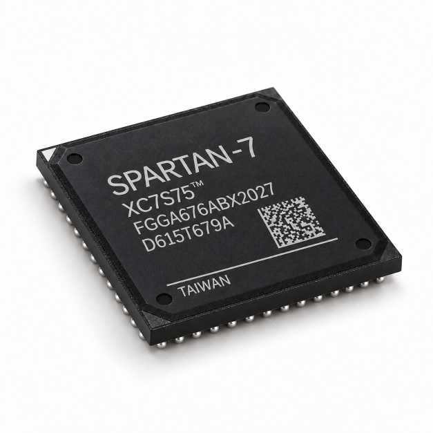
XC7S75-1FGGA676C is a Spartan-7 FPGA with 76,800 logic cells, 3,240 Kb of block RAM, 140 DSP slices, and a maximum of 400 user I/Os in a 676-ball BGA package. It is worth considering when your design requires a large amount of programmable logic and parallel I/O without dedicated multi-gigabit transceivers.
Selecting XC7S75-1FGGA676C involves more than matching resource totals. Your implemented design must fit its logic and memory resources, meet timing with the -1 speed grade, and work within the package’s pin assignments and commercial temperature range. The following sections explain how to evaluate those requirements before committing the device to your PCB and BOM.
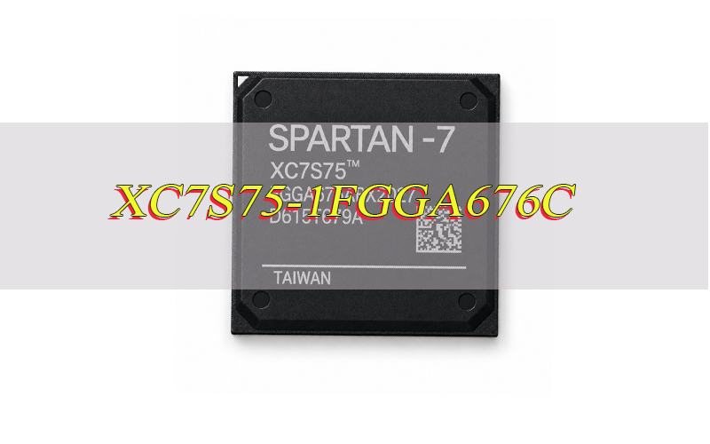
What Does the XC7S75-1FGGA676C Ordering Code Tell You?
The complete ordering code identifies the device, speed grade, package, and temperature grade. These details determine which part you select in Vivado, which footprint and pinout you use, and which operating limits apply.
- XC7S75: Spartan-7 FPGA device designation.
- -1: Speed grade used for electrical timing specifications.
- FGGA676: Package designation for the 676-ball BGA.
- C: Commercial temperature grade.
Record XC7S75-1FGGA676C in your BOM, approved component list, and RFQ. Using only “XC7S75” leaves the package, speed, and temperature requirements unspecified, which can lead to an offer for a different variant.
Which XC7S75-1FGGA676C Specifications Matter Most?
Resource capacity, available I/O, package dimensions, speed grade, and junction temperature are the starting points for selection. Compare each specification with an actual design requirement rather than treating it as an isolated performance figure.
| Specification | XC7S75-1FGGA676C | What to Check |
|---|---|---|
| Logic cells | 76,800 | Whether the implemented logic fits with room for revisions |
| CLB slices | 12,000 | LUT and register utilization in the implementation reports |
| Block RAM | 3,240 Kb | Buffer capacity, memory organization, and port requirements |
| DSP slices | 140 DSP48E1 slices | Arithmetic demand and how synthesis maps the design |
| Maximum user I/O | 400 in FGGA676 | Usable signal assignments, bank voltages, and interface restrictions |
| Package | FGGA676, 27 × 27 mm, 1.0 mm ball pitch | PCB area, escape routing, and assembly requirements |
| Speed grade | -1 | Timing results for the selected device and operating conditions |
| Commercial junction temperature | 0°C to 85°C | Thermal performance across the intended operating environment |
| Dedicated GT transceivers | None | Whether the design requires multi-gigabit serial connectivity |
Logic cells are a normalized capacity figure, not a count of directly assignable LUTs. For a practical comparison, review LUTs, registers, block RAM, and DSP usage separately. Likewise, 400 is the maximum user I/O count for this device-package combination; it does not mean every interface can use any available signal pin.
How Much FPGA Resource Margin Should You Leave?
There is no universal utilization percentage that guarantees a successful XC7S75 implementation. A design with unused logic can still encounter a block RAM shortage, limited DSP capacity, or routing congestion. Evaluate each resource separately and review the result after placement and routing.
Begin with a representative design that includes the intended interfaces, clocking, buffers, and processing functions. Check how synthesis maps arithmetic and memory structures, then compare the implemented utilization with the features you expect to add. Include debug cores and monitoring logic when they will remain in the final design.
For block RAM, total capacity is only part of the decision. Memory width, depth, port arrangement, and the number of independent buffers affect how efficiently the available blocks are used. DSP demand also depends on arithmetic width and whether operations are mapped into DSP48E1 slices or implemented in logic.
XC7S75 remains a suitable option when the representative design fits, routes successfully, and leaves practical room for planned changes. If one resource remains close to its limit after reasonable optimization, compare a larger device such as XC7S100. Check the exact package and migration requirements before treating it as a replacement.
Does the FGGA676 Package Fit Your PCB and I/O Plan?
FGGA676 is suitable when both the signal assignments and the physical PCB layout support your design. Its 1.0 mm ball pitch and 27 × 27 mm body size provide useful starting dimensions, but they do not determine the required layer count or via structure on their own.
Build the I/O plan before completing the schematic. Group interfaces by voltage and I/O standard, assign clocks to appropriate clock-capable pins, and reserve the required differential pairs. Review memory interfaces early because their placement rules can constrain the remaining assignments.
Check these areas together:
- Bank compatibility: Confirm that signals sharing a bank can operate with the selected VCCO and applicable reference-voltage requirements.
- Special-purpose pins: Check clock, configuration, analog, and other dedicated functions before assigning general signals.
- Interface placement: Verify differential-pair locations and memory-interface assignments against the exact device pinout.
- PCB escape routing: Confirm that fabrication rules, vias, layer allocation, and power distribution support the proposed fanout.
The 676-ball designation does not represent 676 general-purpose I/Os. Use the XC7S75 FGGA676 pinout rather than copying assignments from another device with the same ball count. Check both the package pin map and I/O-bank information before completing the schematic.
Is the -1 Speed Grade Fast Enough for Your Design?
The -1 speed grade is sufficient when the fully constrained implementation meets internal and external timing requirements with usable margin. It does not correspond to one fixed maximum clock frequency. A simple pipeline and a long combinational path can produce very different timing results on the same FPGA.
Use XC7S75-1FGGA676C as the target device in Vivado, then review timing after placement and routing. Check setup and hold results, generated clocks, input and output delays, and any unconstrained paths. A passing result is meaningful only when the constraints describe the real clocks and connected interfaces.
When timing fails, determine whether the cause is the logic architecture, routing, clocking, or constraints. Pipelining, reducing fan-out, or changing placement may resolve a problem without changing the device. Clock-domain crossings also require appropriate design treatment; selecting a faster grade does not make an unsafe crossing reliable.
Compare the -2 grade when the design still misses required timing after those issues have been addressed. The -2 grade offers higher performance within the Spartan-7 family, but its benefit for your design should be confirmed through implementation.
Can the Commercial Temperature Grade Handle Your Operating Environment?
XC7S75-1FGGA676C is rated for a junction temperature of 0°C to 85°C. This is the temperature inside the operating device, not the temperature of the room or enclosure. A board operating in moderate ambient conditions can still exceed the limit if FPGA power and heat removal are poorly balanced.
Estimate power using the intended clocks, resource utilization, and switching activity. Then evaluate enclosure temperature, airflow, nearby heat sources, and the thermal path through the package and PCB. Validate the estimate on representative hardware across the expected operating conditions.
Controlled indoor equipment may suit the commercial grade when testing demonstrates sufficient thermal margin. Outdoor equipment, cold-start applications, and hot industrial enclosures may call for a wider temperature range. Industrial-grade Spartan-7 devices have a specified junction-temperature range of −40°C to 100°C.
Changing the temperature suffix should follow a documented component review. Confirm the exact ordering code, applicable specifications, availability, and project approval requirements before updating the BOM.
What Power and Configuration Requirements Should You Check?
Your PCB must provide the correct FPGA supplies and a configuration circuit that supports reliable startup. Review these requirements before layout because regulator selection, bank voltages, and configuration connections can affect component placement and routing.
The supply plan should account for VCCINT, VCCBRAM, VCCAUX, and VCCO, together with any additional supplies required by the functions you use. Size the regulators from a design-based power estimate and check voltage tolerance, transient response, and decoupling. VCCO must match the interfaces assigned to each bank.
Review power sequencing as well as steady-state voltage. AMD recommends powering VCCINT, VCCBRAM, VCCAUX, and then VCCO. Rails with compatible requirements may be powered together under the conditions described in DS189.
For configuration, confirm the supported boot mode, configuration-memory compatibility, and sufficient storage for the intended bitstream arrangement. Reserve practical JTAG access and check the mode pins and configuration-bank requirements against the official documentation.
For an existing PCB, compare these circuits before approving a device change. Matching package dimensions alone does not establish that the regulators, bank voltages, or configuration hardware will support the proposed FPGA.
Why Source XC7S75-1FGGA676C Through Melson Components?
Once the design is approved, the supplied material should match the complete BOM requirement. Melson Components supports buyers with part identification, quantity confirmation, packaging review, and project-specific inspection arrangements.
- Exact part matching: Check the offered speed grade, package, and temperature grade against XC7S75-1FGGA676C.
- Quantity and delivery confirmation: Verify the quantity available for your order and the proposed shipping schedule.
- date code and lot code review: Compare the offered material, labels, and records with your acceptance requirements.
- Packaging review: Check available packaging and identification information before shipment.
- Inspection options: Visual inspection, X-Ray, De-Cap, or functional testing can be arranged according to the agreed scope and acceptance criteria.
- Traceability records: RFQ, inspection, packing, and shipping records can be retained for up to 15 years.
Send the exact part number, quantity, date code requirement, and delivery location to sales@melsonchip.com. Include any packaging, inspection, traceability, or no-substitution requirements so the quotation reflects the material you can accept.
FAQs About XC7S75-1FGGA676C
Q1: Where can I find the XC7S75-1FGGA676C datasheet?
A1: Use AMD’s DS180 device overview for resources and package combinations, and DS189 for electrical limits and timing specifications.
Q2: Where can I find the FGGA676 pinout?
A2: Use AMD’s UG475 packaging and pinout guide. Select the information for XC7S75 in FGGA676 and confirm that your schematic symbol matches it.
Q3: Does XC7S75-1FGGA676C contain an embedded processor?
A3: It does not contain a hard processor subsystem like a Zynq device. You can implement a MicroBlaze soft processor in its programmable logic, with resource usage depending on the processor configuration and connected peripherals.
Q4: Does XC7S75 include an XADC?
A4: Yes. XC7S75 includes one XADC block. Check its analog-input connections and operating requirements before using it for external measurements or device monitoring.
Q5: Does XC7S75 have a hard PCIe block or dedicated GT transceivers?
A5: No. The official device overview lists neither for XC7S75. Designs requiring these resources should compare another FPGA family.
Q6: Can XC7S75-1FGGA676C be used with DDR3 memory?
A6: Yes, DDR3 interfaces can be implemented using the supported Vivado Memory Interface Generator (MIG) flow. Select XC7S75-1FGGA676C in the tool and validate the memory type, interface width, data rate, and pin assignments before finalizing the PCB.
Q7: Can the same bitstream be used for XC7S75 and XC7S100?
A7: No. Generate a separate bitstream for each target device. Moving the design from XC7S75 to XC7S100 requires implementation and timing verification for XC7S100, even when the selected packages support PCB migration.
Q8: Does a larger package provide more FPGA logic?
A8: No. FPGA resource capacity depends on the device, while the package determines its physical footprint and available connections. XC7S75 has the same logic, block RAM, and DSP resources in FGGA484 and FGGA676, but FGGA676 provides more user I/O connections.
Conclusion
XC7S75-1FGGA676C is a suitable choice when your implemented design fits its resources, meets timing with the -1 grade, and works within the FGGA676 pinout and commercial junction-temperature limits. Confirm those results alongside the power and configuration circuits before finalizing the PCB. Resource totals alone cannot establish whether the complete design will work.
If XC7S75-1FGGA676C is already approved for your project, contact Melson Components at sales@melsonchip.com to check quantity, delivery, date code, packaging, and inspection options. Provide your acceptance requirements with the RFQ so the offered material can be reviewed against the approved BOM.