 English
 中文
 english


Selecting XC7A100T-2FGG484I involves more than checking logic capacity. The package, available I/O, GTP channels, speed grade, temperature grade, PCB requirements, power design, and supply conditions all affect whether the device fits a project.
For engineering and purchasing teams, the most useful approach is to confirm these factors in sequence. This guide explains what to check in the datasheet, how to judge whether FGG484 fits the design, when another XC7A100T variant makes more sense, and what to verify before buying the part.
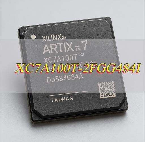
What Should You Check in the XC7A100T-2FGG484I Datasheet Before Selection?
Before selecting XC7A100T-2FGG484I, start with the specifications that directly affect design compatibility. In the full part number, XC7A100T identifies the device, -2 is the speed grade, FGG484 is the package, and I indicates the industrial temperature grade.
The table below summarizes the main XC7A100T-2FGG484I specifications to review before comparing it with other FPGA options.
| Specification | XC7A100T-2FGG484I |
|---|---|
| Device family | Artix-7 FPGA |
| Logic cells | 101,440 |
| Block RAM | 4,860 Kb |
| DSP48E1 slices | 240 |
| User I/O in FGG484 | 285 |
| GTP transceivers in FGG484 | 4 |
| Clock management tiles | 6 |
| Package | FGG484, 23 × 23 mm, 1.0 mm pitch |
| Speed grade | -2 |
| Temperature grade | Industrial, -40°C to +100°C junction range |
These values show whether the part is a realistic candidate, but they do not confirm that it will work in a specific design. Resource utilization, pin assignment, serial interfaces, timing, PCB layout, power, and thermal performance still need to match the released product design. If you want to learn more information about XC7A100T-2FGG484I datasheet before selection, please refer to the following pdf:
Does XC7A100T-2FGG484I Have Enough Logic, BRAM, and DSP Resources?
XC7A100T provides 101,440 logic cells, 4,860 Kb of block RAM, and 240 DSP48E1 slices. Whether those resources are sufficient depends on the implemented design rather than the headline capacity alone.
The resource report should reflect the complete design, including final IP, LUT and flip-flop use, BRAM mapping, DSP usage, debug logic, routing congestion, and timing. An early RTL estimate may look comfortable while the final routed design leaves little margin.
A practical decision is straightforward:
- Keep XC7A100T-2FGG484I if the complete design fits, routes, and meets timing with reasonable margin.
- Review the implementation if required functions are still missing from the build.
- Compare a higher-capacity FPGA if the design only fits after removing required functionality or repeatedly fails placement and routing.
For production projects, do not select the device solely because the nominal resource count appears large enough.
Can FGG484 Support Your I/O and High-Speed Interfaces?
For XC7A100T, the FGG484 package provides 285 user I/Os and four GTP transceiver channels. These numbers are more useful than the total 484-ball count when deciding whether the package can support the board.
The approved pin map should account for I/O-bank voltages, differential pairs, clock-capable pins, configuration pins, reference clocks, and GTP locations. Even when the total I/O count appears sufficient, signals cannot always be moved freely between banks.
The same applies to high-speed interfaces. Four GTP channels are sufficient only when the design requires no more than four bonded serial lanes and the required reference-clock arrangement works with the selected package.
If the design needs more bonded I/O or additional GTP channels, XC7A100T-2FGG676I is one alternative to compare. It provides more package resources, but moving from FGG484 to FGG676 also changes the footprint and requires another PCB review.
Is the FGG484 Package Practical for Your PCB Design?
FGG484 is a 23 × 23 mm, 1.0 mm pitch BGA package. The package itself is not unusually difficult for a capable multilayer PCB process, but whether it is practical depends on the board stackup, fan-out strategy, routing density, and assembly requirements.
Before fixing the device in the BOM, review:
- land pattern and footprint compatibility;
- stackup and via structure for BGA escape routing;
- power and ground connections;
- decoupling placement;
- hidden-joint inspection requirements;
- any additional PCB layers or process steps caused by the package.
A larger package may provide more accessible I/O and GTP resources, but it can also increase PCB area, routing changes, assembly cost, and qualification work.
For this reason, package selection should be based on the total board impact, not just the FPGA unit price.
Do the -2 Speed Grade and Industrial Temperature Grade Fit Your Design?
The -2 speed grade should be used only when the released design meets timing at that grade. Post-route verification should confirm setup, hold, interface timing, and all constrained clock paths.
A different speed grade should not be substituted simply because it is cheaper or easier to source. Changing from -2 to another grade changes the timing basis of the design and should be revalidated before the BOM is changed.
The final I suffix identifies the industrial temperature grade, with a junction-temperature range of -40°C to +100°C. This is a silicon junction limit rather than an ambient-temperature specification.
Thermal evaluation should therefore consider FPGA power, PCB heat transfer, enclosure temperature, airflow, and nearby heat sources. A commercial-temperature alternative should not be treated as equivalent unless the product’s operating and qualification requirements allow the change.
Can Your Power and Configuration Design Support XC7A100T-2FGG484I?
XC7A100T-2FGG484I is an SRAM-based FPGA, so the board must provide the correct power architecture and a reliable configuration path.
The design should cover core, auxiliary, BRAM, I/O-bank, and GTP supplies, along with startup behavior, voltage tolerance, decoupling, and expected power dissipation. Power planning should reflect the actual FPGA workload rather than nominal device values alone.
Configuration also needs to be defined before production. The product should have a tested method for:
- loading the FPGA image at power-up;
- programming through JTAG;
- updating the image when required;
- recovering from an interrupted or failed update.
If the power rails or configuration path are still unresolved, the FPGA selection is not ready for production.
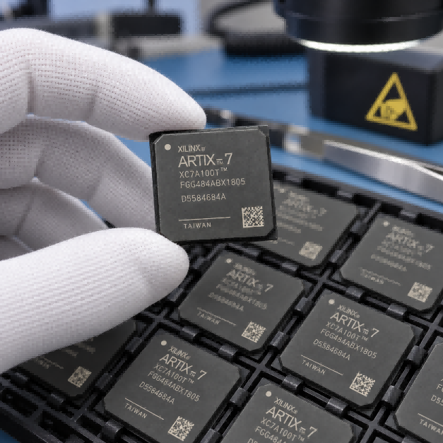
When Should You Choose Another XC7A100T Variant Instead?
Another XC7A100T variant is worth considering when XC7A100T-2FGG484I cannot meet the required I/O, GTP, timing, package, or cost target. Parts in the same XC7A100T family are not automatically interchangeable, so compare the exact OPN before changing the BOM.
The table below compares several relevant options and the situations in which each one may fit better.
| Part Number | Main Difference | When It May Fit Better |
|---|---|---|
| XC7A100T-2FGG484I | 285 user I/Os, four GTP, -2, industrial grade | Current design and PCB already fit FGG484 |
| XC7A100T-2FGG676I | Larger package with more bonded I/O and GTP access | More I/O or serial lanes are required |
| XC7A100T-1FGG484I | Same device and package, slower -1 grade | The design passes timing at -1 and the change improves cost or availability |
| XC7A75T-2FGG484I | Lower logic density | The complete design fits the smaller FPGA with sufficient margin |
Do not compare only the component price. PCB changes, engineering time, qualification, testing, and schedule impact can easily outweigh a lower FPGA unit cost.
What Should You Check Before Buying XC7A100T-2FGG484I?
Once engineering has approved the part, supplier quotations should be compared using the same exact OPN, quantity, delivery requirement, and quality conditions. Otherwise, two offers may appear similar while covering different lots, packaging conditions, or inspection scopes.
Before placing the order, check:
- Exact OPN and no substitution: The quotation and purchase order should state XC7A100T-2FGG484I. Any change to the device, speed grade, package, or temperature grade should require approval.
- Required quantity and allocable stock: Confirm how many pieces can actually be allocated to the order. An online inventory figure does not prove that the required quantity is available from the same lot or ready to ship.
- Price and total purchase cost: Compare unit price, quantity breaks, testing charges, freight, duties, and other costs rather than unit price alone.
- Lead time and committed delivery: Request a dated quotation showing the confirmed ship date, material location, and delivery destination.
- Date code, lot, and packaging: Confirm the acceptable date-code range, whether the quantity is from one or multiple lots, packaging condition, moisture protection, and any repackaging.
- Traceability and inspection evidence: Define the required documentation and test scope. Depending on the project, this may include visual inspection, marking and label verification, X-ray, De-Cap, electrical testing, or functional testing.
If the lot, date code, quantity, inspection result, or proposed part changes before shipment, review the exception before the order proceeds.
Why Choose Melson Components for XC7A100T-2FGG484I Sourcing?
When XC7A100T-2FGG484I is difficult to source, buyers need more than a stock figure. The useful question is whether the offered quantity, lot, date code, packaging, inspection scope, and delivery can match the actual build requirement.
Melson Components supports buyers with:
- Visual inspection, X-ray, De-Cap, and functional testing when required
- Sourcing, inspection, packing, and shipment records retained for up to 15 years
- BOM reviews covering availability, lead time, EOL, and alternative-part risks
- lot and source documentation for purchasing and quality review
- alternative sourcing support when the original FPGA becomes constrained
These capabilities allow purchasing teams to compare availability, lot condition, quality evidence, and delivery before committing the material to production.
Would you like to get a faster quote for XC7A100T-2FGG484I? Send your required quantity, date code requirement, and delivery location to sales@melsonchip.com. We can check available supply, lot information, pricing, and delivery options against your requirement.
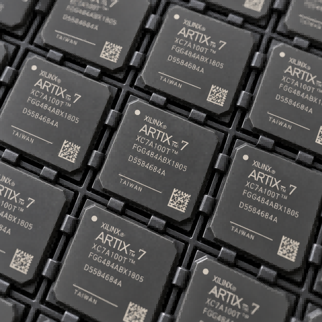
FAQs About Selecting XC7A100T-2FGG484I
Q1: Is XC7A100T-2FGG484I suitable for a new FPGA design?
A1: It can be when the required logic, BRAM, DSP, I/O, GTP, timing, power, and thermal requirements fit the device. Supply availability and product lifecycle should also be considered before committing to long-term production.
Q2: Does FGG484 provide 484 usable I/O pins?
A2: No. XC7A100T in the FGG484 package provides 285 user I/Os. The remaining balls are used for power, ground, configuration, transceiver, and other dedicated functions.
Q3: When should XC7A100T-2FGG676I be considered instead?
A3: Consider it when the design requires more bonded user I/O or more GTP channels than FGG484 provides. The larger package also requires a footprint and PCB review.
Q4: Can XC7A100T-1FGG484I replace the -2 version?
A4: Only if the released design passes timing at the -1 speed grade and the BOM change is approved.
Q5: Is the I suffix an ambient-temperature rating?
A5: No. It identifies the industrial junction-temperature grade. Actual junction temperature depends on power dissipation, PCB thermal performance, airflow, and the product environment.
Q6: Can older-date-code XC7A100T-2FGG484I parts still be used?
A6: They can be acceptable when storage history, packaging, moisture control, traceability, and any required solderability or functional testing meet the project’s requirements.
Q7: Does X-ray inspection alone prove an FPGA is authentic?
A7: No. X-ray is one inspection method. Traceability, package markings, labels, physical inspection, and electrical or functional testing may also be required depending on sourcing risk.
Q8: What should you do if the tray label and device markings do not match?
A8: Hold the lot before assembly. Review the packaging, traceability, lot records, and component markings and release the material only after the discrepancy has been resolved.