 English
 中文
 english


The XC7A100T-2CSG324I is an industrial-grade Artix-7 FPGA with 101,440 logic cells, 240 DSP48E1 slices, 4,860 Kb of block RAM, and 210 user I/Os in the CSG324 package. It combines programmable logic, DSP, embedded memory, clock resources, and configurable I/O in a compact 15 × 15 mm BGA package.
Selecting this FPGA requires more than checking logic density. The CSG324 package determines the I/O and interface resources physically available to the design, while the -2 speed grade and industrial temperature suffix affect timing and operating conditions. This guide covers the XC7A100T-2CSG324I datasheet, pinout, power and configuration requirements, applications, selection points, and purchasing checks.
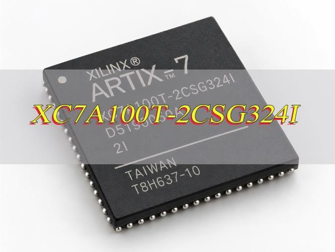
What Is the Xilinx XC7A100T-2CSG324I?
The XC7A100T-2CSG324I is a 101,440-logic-cell Artix-7 FPGA in a CSG324 package with a -2 speed grade and industrial temperature rating. The device also provides 15,850 CLB slices, 240 DSP48E1 slices, 4,860 Kb of block RAM, six clock management tiles, and an integrated XADC.
This resource mix supports control logic, parallel processing, buffering, arithmetic operations, signal processing, and custom digital interfaces within one programmable device. Compared with lower-density Artix-7 parts, the XC7A100T provides more logic, DSP, and memory capacity for designs that need additional processing headroom.
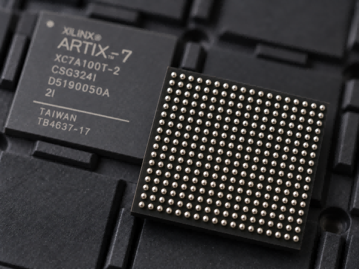
The CSG324 package provides 210 user I/Os with a 15 × 15 mm body size and 0.8 mm ball pitch, but it does not expose the GTP transceivers available through some larger XC7A100T packages. XC7A100T-2CSG324I is therefore best viewed as an Artix-7 option focused on programmable logic, DSP, embedded memory, and parallel I/O rather than dedicated multi-gigabit serial connectivity.
What Does the XC7A100T-2CSG324I Part Number Mean?
The full XC7A100T-2CSG324I ordering code identifies the device, speed grade, package, and temperature grade. These suffixes affect timing, PCB compatibility, available package resources, and operating conditions, so the complete part number should remain intact during both design and procurement.
- XC7A100T identifies the Artix-7 XC7A100T FPGA.
- -2 identifies the speed grade.
- CSG324 identifies the 324-ball CSG package.
- I identifies the industrial temperature grade.
The industrial version is specified for a -40°C to +100°C junction temperature range. This makes the “I” suffix relevant for industrial equipment, instrumentation, outdoor electronics, and other applications that may operate outside commercial temperature limits.
A device such as XC7A100T-2CSG324C or an XC7A100T in FGG484 should therefore not automatically be treated as equivalent to XC7A100T-2CSG324I. The base FPGA may be related, but the temperature grade, package footprint, pinout, and available resources can differ.
What Are the Main XC7A100T-2CSG324I Datasheet Specifications?
The XC7A100T-2CSG324I provides 101,440 logic cells, 240 DSP48E1 slices, 4,860 Kb of block RAM, 210 user I/Os, and no exposed GTP transceivers in CSG324. These are the first specifications to check when deciding whether this exact device-package combination fits a design.
| Parameter | XC7A100T-2CSG324I |
|---|---|
| Family | Artix-7 |
| Logic cells | 101,440 |
| CLB slices | 15,850 |
| Distributed RAM | 1,188 Kb |
| DSP48E1 slices | 240 |
| Block RAM | 4,860 Kb |
| Block RAM blocks | 135 × 36 Kb / 270 × 18 Kb |
| Clock management tiles | 6 |
| XADC blocks | 1 |
| User I/O | 210 |
| GTP transceivers | 0 in CSG324 |
| Package | CSG324 |
| Package size | 15 × 15 mm |
| Ball pitch | 0.8 mm |
| Speed grade | -2 |
| Temperature grade | Industrial |
| Junction temperature | -40°C to +100°C |
One specification deserves particular attention: CSG324 provides 210 user I/Os but does not expose the XC7A100T GTP transceivers. Device-level XC7A100T specifications may show higher maximum I/O counts and GTP capability because those figures include other package combinations.
For initial selection, use the package-specific XC7A100T-2CSG324I values rather than the maximum XC7A100T family figures. If dedicated multi-gigabit serial transceivers are required, another XC7A100T package should be evaluated before the schematic is fixed.
If you want to know more about the datasheet of XC7A100T-2CSG324I, please refer to the following pdf file:
How Is the XC7A100T-2CSG324I Pinout Organized?
The XC7A100T-2CSG324I pinout is divided among banked user I/O, clock-capable pins, power and ground connections, configuration signals, JTAG, XADC pins, and other dedicated or multifunction pins. The 324 physical balls should therefore not be interpreted as 324 general-purpose I/Os.
The main pin groups are:
- User I/O pins for external digital interfaces.
- Clock-capable pins for signals that require dedicated clock routing.
- Power and ground pins for core, auxiliary, memory, I/O-bank, and analog supplies.
- Configuration pins for startup and bitstream loading.
- JTAG pins for configuration, boundary scan, and debugging.
- XADC pins for analog monitoring and measurement.
- Dedicated or multifunction pins whose function can change between configuration and normal operation.
The 210 available user I/Os are distributed across package-specific I/O banks, and not every XC7A100T bank is fully available in CSG324. Signal assignment should therefore be based on the official CSG324 pinout rather than a generic Artix-7 bank diagram or the total ball count.
Which I/O and Clock Pins Matter Most in the XC7A100T-2CSG324I Pinout?
Three checks matter most when assigning XC7A100T-2CSG324I I/O and clock pins: I/O-bank voltage compatibility, clock-capable pin placement, and valid differential-pair assignment. Having fewer than 210 external signals does not guarantee that every interface can be placed successfully.
- I/O-bank voltage: signals within a bank must be compatible with its VCCO supply and supported I/O standards.
- Clock-capable pins: system clocks and timing-sensitive inputs should use suitable clock-capable locations.
- Differential pairs: differential interfaces must use valid complementary pin pairs rather than arbitrary general-purpose I/Os.
Bank planning becomes particularly important when the FPGA connects to devices operating at several voltage levels. A design may have enough I/O numerically but still fail pin planning if incompatible interfaces compete for the same bank resources. Clock-capable pins should also be reserved before general-purpose assignments are finalized, while differential signals must remain on supported pairs.
A valid pin plan therefore depends on bank voltage, pin function, clock capability, and differential pairing—not simply total I/O count. Completing these checks before PCB layout reduces the risk of late signal reassignment or board changes.
What Power and Configuration Requirements Should You Check?
The XC7A100T-2CSG324I requires separate core, block-RAM, auxiliary, I/O-bank, and analog-related power connections, while configuration relies on dedicated startup and programming signals. Power architecture and configuration strategy should therefore be defined before the schematic is released.
The main supplies include:
- VCCINT for FPGA core logic.
- VCCBRAM for block RAM.
- VCCAUX for auxiliary circuitry.
- VCCO for individual I/O banks.
- Ground and analog-related connections required by the device.
For the standard -2 device, VCCINT and VCCBRAM are nominally 1.0 V, while VCCAUX uses the specified auxiliary supply and VCCO depends on the I/O standards assigned to each bank. Actual current demand varies with logic utilization, clock frequency, DSP activity, block RAM use, I/O switching, and temperature, so regulator capacity and decoupling should be based on the implemented design rather than the part number alone.
Configuration should be planned at the same stage. Confirm the boot source, configuration mode, required configuration memory, programming connections, JTAG access, startup signals, and pull-resistor requirements before schematic release. Finalizing the power and configuration architecture together reduces the chance that either one forces late changes to the PCB or pin assignment.
What Applications Use the XC7A100T-2CSG324I?
The XC7A100T-2CSG324I is suited to designs that require approximately 100K Artix-7 logic cells, substantial DSP and block RAM resources, parallel I/O, and industrial-temperature operation without package-level GTP connectivity.
Typical applications include:
- Industrial automation and control: programmable logic can handle deterministic control, encoder processing, custom timing, interface management, and parallel I/O.
- Data acquisition: 240 DSP48E1 slices and 4,860 Kb of block RAM can support filtering, arithmetic processing, buffering, and multi-channel data handling.
- Machine vision and imaging: the FPGA can manage synchronization, buffering, interface control, data formatting, and image preprocessing.
- Instrumentation and test equipment: configurable logic, internal memory, clock resources, and wide I/O support measurement and signal-processing systems. The integrated XADC can also monitor device temperature, supply voltages, and selected low-speed analog signals.
- Embedded digital systems: FPGA logic can offload parallel, timing-sensitive, or custom hardware functions from a processor or microcontroller.
- Interface and communication equipment: the device can implement protocol conversion, framing, buffering, and parallel interfaces where dedicated GTP links are not required.
These application categories indicate where the resource mix can be useful, but they do not determine suitability by themselves. The final choice depends on whether the required logic, DSP, memory, I/O banks, clocking, timing, and interface resources fit the exact CSG324 implementation.
How Do You Know Whether XC7A100T-2CSG324I Fits Your Application?
The XC7A100T-2CSG324I fits a design only when its logic, DSP, memory, I/O, clocking, package, timing, and temperature resources satisfy the same implementation. A sufficient logic-cell count cannot compensate for an incompatible I/O-bank plan or a required interface that is not available in CSG324.
Evaluate the device against these requirements:
- Logic capacity: estimate LUT, register, and routing use with margin for later revisions.
- DSP demand: compare arithmetic and filtering workloads with the 240 DSP48E1 slices.
- Internal memory: check buffering and storage requirements against 4,860 Kb of block RAM and 1,188 Kb of distributed RAM.
- I/O requirement: compare actual signal count and bank distribution with the 210 available user I/Os.
- Clocking: reserve suitable clock-capable pins and verify the required clock architecture.
- Serial connectivity: select another package if the system requires GTP transceivers.
- PCB constraints: confirm that the 15 × 15 mm, 0.8 mm-pitch BGA matches the stackup, breakout strategy, and assembly capability.
- Timing: verify the implemented design against the -2 speed-grade timing requirements.
- Temperature: confirm that the industrial -40°C to +100°C junction range matches the expected operating environment.
Complete these checks before the PCB footprint is fixed. If the I/O-bank plan fails, GTP connectivity is required, or a major FPGA resource is already close to its limit, evaluate another package or device before PCB layout begins. Changing packages later can affect the footprint, pin assignment, bank structure, and available interfaces.
What Should You Verify Before Ordering XC7A100T-2CSG324I?
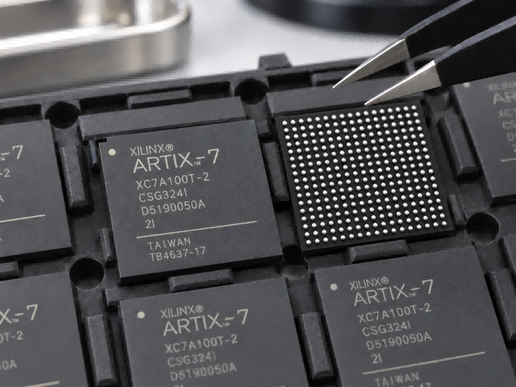
Before ordering XC7A100T-2CSG324I, verify the complete MPN, quantity, package, speed grade, temperature suffix, date code requirement, lot conditions, packaging, traceability, and inspection scope. Procurement should not approve a quotation simply because it contains the XC7A100T base number.
Confirm the following:
- Exact MPN: XC7A100T-2CSG324I.
- Manufacturer: AMD/Xilinx.
- Package: CSG324.
- Speed grade: -2.
- Temperature grade: I.
- Quantity: prototype, pilot, or production volume.
- date code requirement: state any project restrictions.
- lot code requirement: define whether mixed lots are acceptable.
- Packaging: confirm packaging and moisture-protection requirements.
- Traceability: define the records required for the supplied lot.
- Inspection/testing: specify whether visual inspection, X-Ray, De-Cap, functional testing, or another agreed method is required.
An online inventory quantity does not prove that the same physical lot will be supplied. Before releasing the purchase order, confirm that the exact MPN, quantity, label photographs, date code/lot code, packaging, inspection records, traceability requirements, and delivery terms all refer to the same offered lot. Compare quotations on this basis rather than on unit price alone.
Why Source XC7A100T-2CSG324I From Melson Components?
When sourcing XC7A100T-2CSG324I, buyers need more than price and availability. Melson Components helps reduce sourcing risk through inspection, traceability, supply support, and requirement-based verification.
- Reduce Incoming Quality Risk
Support visual inspection, X-Ray, De-Cap, LCR, and functional testing based on the agreed scope, helping you verify the supplied lot before production. - Maintain Long-Term Traceability
RFQ, sourcing, inspection, packing, and shipment records can be retained for up to 15 years, making later quality reviews easier to trace. - Reduce Supply Disruption
Support sourcing for shortage, long lead-time, and EOL components, helping you respond earlier when availability changes. - Avoid Incorrect Substitutions
Your RFQ can lock the required CSG324 package, -2 speed grade, industrial temperature grade, date code, and no-substitution condition to reduce compatibility risk.
For an XC7A100T-2CSG324I RFQ, send your quantity, date code requirement, delivery location, and inspection or testing requirements to sales@melsonchip.com.
FAQ About XC7A100T-2CSG324I
The questions below cover Vivado support, XADC, Device DNA, configuration security, Dynamic Function eXchange, DDR3, and block RAM ECC, adding details not repeated in the main sections above.
Q1: Does Vivado still support XC7A100T-2CSG324I?
A1: Yes. XC7A100T remains supported by current AMD Vivado tools, allowing engineers to synthesize, implement, and generate bitstreams for the device. When migrating an older project, check IP versions, constraints, and timing results before rebuilding it in a newer Vivado release.
Q2: Does XC7A100T-2CSG324I include a built-in ADC?
A2: Yes. The XC7A100T includes the 7 Series XADC with two 12-bit ADCs, which can monitor internal conditions and selected external analog inputs. It is useful for voltage monitoring, temperature sensing, and lower-speed analog measurement.
Q3: Can the XADC replace an external high-speed ADC?
A3: Not for most high-speed acquisition systems. The integrated XADC operates at up to about 1 MSPS, making it suitable for monitoring and lower-speed measurements but below the sampling rates required by many RF, imaging, and high-speed acquisition systems.
Q4: Can XC7A100T monitor its own temperature and supply voltages?
A4: Yes. The integrated XADC can monitor FPGA die temperature and internal supply voltages, providing useful operating data for board bring-up, thermal management, and system diagnostics.
Q5: Can the XADC sample two analog inputs simultaneously?
A5: Yes. Its dual-ADC architecture supports simultaneous sampling modes. The available channels and external connections still need to be checked against the CSG324 pinout and board-level analog design.
Q6: Does XC7A100T have a device identification feature?
A6: Yes. Artix-7 devices include Device DNA, providing device-identification information accessible through FPGA logic or JTAG. It can support board tracking, product identification, licensing, and system-level asset management.
Q7: Can the XC7A100T-2CSG324I configuration bitstream be encrypted?
A7: Yes. 7 Series FPGAs support configuration-security functions for protecting FPGA bitstreams. If security is required, key handling, production programming, field updates, and recovery procedures should be defined before volume production.
Q8: Does XC7A100T support partial reconfiguration?
A8: Yes. XC7A100T supports Dynamic Function eXchange (DFX), formerly called partial reconfiguration. This allows selected FPGA regions to be updated while the static portion of the design continues operating.
Q9: Can XC7A100T-2CSG324I interface with DDR3 memory?
A9: Yes, but DDR3 implementation depends on the CSG324 I/O-bank allocation, pin availability, memory width, clocking, termination, and PCB routing. Validate the intended memory configuration before fixing the PCB pinout.
Q10: Does XC7A100T block RAM support ECC?
A10: Yes. The 7 Series block RAM provides ECC capability in supported memory configurations, allowing error detection and correction in designs that require greater internal-memory reliability.
The XC7A100T-2CSG324I combines 101,440 Artix-7 logic cells, 240 DSP48E1 slices, 4,860 Kb of block RAM, 210 CSG324 user I/Os, a -2 speed grade, and industrial-temperature operation. Its main package limitation is equally clear: CSG324 does not expose the XC7A100T GTP transceivers, so the exact package resources should be confirmed before the device is designed into the board.
If XC7A100T-2CSG324I is already specified in your BOM, send your quantity, date code requirement, delivery location, and inspection or testing requirements to sales@melsonchip.com. Melson Components can support lot verification, inspection, packaging review, and long-term traceability before shipment.