 English
 中文
 english


The XC6SLX16-2CSG324I is a Xilinx Spartan-6 LX FPGA in the CSG324 package with a -2 speed grade and an industrial temperature rating. Before selecting it, the practical questions are whether the available logic, memory, DSP, and I/O resources fit the design, whether timing closes on the -2 device, and whether the package, power, clocking, and configuration requirements match the board.
The XC6SLX16-2CSG324I datasheet is most useful as a selection tool rather than a parameter list. A design can fit the headline logic capacity and still be a poor match because of I/O-bank constraints, insufficient Block RAM, an incompatible power tree, or a development environment that does not fit the Spartan-6 tool flow.
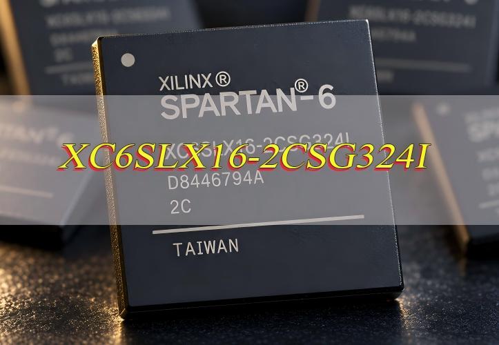
Which XC6SLX16-2CSG324I Specifications Should You Check Before Selection?
Start with logic capacity, memory, DSP resources, user I/O, speed grade, package, temperature range, power rails, and clock/configuration resources. These specifications can quickly show whether the device is worth taking into implementation. Below are the parameter table and datasheet (PDF) for your reference when selecting the XC6SLX16-2CSG324I.
| Parameter | XC6SLX16-2CSG324I | Why It Matters |
|---|---|---|
| Family | Spartan-6 LX | Architecture and tool flow |
| Logic cells | 14,579 | Overall programmable logic capacity |
| Slices | 2,278 | Logic implementation resources |
| Flip-flops | 18,224 | Sequential logic capacity |
| Distributed RAM | 136 Kb | Small local memories |
| Block RAM | 576 Kb | On-chip storage and buffering |
| DSP48A1 slices | 32 | Dedicated arithmetic resources |
| CMTs | 2 | Clock generation and management |
| Maximum MCBs | 2 | External memory controller resources |
| User I/O in CSG324 | 232 | External interface capacity |
| Package | CSG324, 15 × 15 mm, 0.8 mm pitch | Footprint and routing |
| Speed grade | -2 | Timing characteristics |
| Temperature grade | Industrial, Tj -40°C to +100°C | Operating environment |
| GTP transceivers | None | No hard multi-gigabit serial links |
| PCIe endpoint block | None | No hard PCIe endpoint |
AMD/Xilinx lists the XC6SLX16 with 14,579 logic cells, 2,278 slices, 18,224 flip-flops, 136 Kb distributed RAM, 576 Kb Block RAM, 32 DSP48A1 slices, two CMTs, up to two Memory Controller Blocks, four I/O banks, and a maximum of 232 user I/Os. The CSG324 package measures 15 × 15 mm with a 0.8 mm ball pitch and supports up to 232 user I/Os.
The full ordering code matters. XC6SLX16 identifies the FPGA device, -2 is the speed grade, CSG324 identifies the package, and I indicates the industrial temperature grade. DS162 specifies the industrial junction-temperature range as -40°C to +100°C. Matching only “XC6SLX16” is therefore not enough when approving a device for a schematic, BOM, or existing design.
Are the Logic, Memory, DSP, and I/O Resources Enough for Your Design?
They are enough only if the implemented design fits all major resource types with practical margin. The XC6SLX16-2CSG324I offers a balanced mix of general logic, embedded memory, DSP, and I/O, but the limiting resource depends on the project.
Logic-heavy control, bridging, and state-machine designs may become constrained by slices, flip-flops, or routing before Block RAM is exhausted. Designs with FIFOs, lookup tables, packet buffers, or embedded data storage can instead reach the 576 Kb Block RAM limit first. Arithmetic-heavy processing can consume the 32 DSP48A1 slices while substantial general-purpose logic remains available.
The same applies to I/O. CSG324 gives XC6SLX16 up to 232 user I/Os, but bank voltages, differential pairs, clock-capable pins, VREF requirements, and configuration functions determine how many pins are actually usable for a specific interface plan.
The XC6SLX16/CSG324 combination also supports two Memory Controller Blocks (MCBs). These dedicated blocks support approved external memory configurations, including DDR, DDR2, DDR3, and LPDDR, which can reduce the programmable logic needed for memory control. The memory type, bus width, pin group, and supported MCB configuration still have to match the actual design.
For a selection decision, compile the real design for the exact XC6SLX16-2CSG324I target and review post-implementation utilization. An RTL estimate may look comfortable but become much tighter after routing, I/O assignment, memory placement, and timing constraints are applied.
Will the -2 Speed Grade Meet Your Timing Requirements?
The -2 speed grade is suitable only when the implemented design meets its required timing on the -2 timing model. It is not a single maximum-frequency specification for the entire FPGA.
Actual performance depends on the paths created by the design: logic depth, routing delay, Block RAM access, DSP paths, clock distribution, and external I/O timing all contribute. Two products built around the same XC6SLX16-2CSG324I can therefore have very different achievable clock rates.
Use the exact -2 target, apply the real clock and I/O constraints, and check setup and hold timing after place and route. DS162 notes that the timing characteristics of an industrial -2 Spartan-6 device are the same as those of the corresponding -2 commercial device.
If a design fails timing on -2, unused logic capacity does not solve the problem. Resource capacity tells you whether the design can fit; the speed grade tells you whether it can run at the required timing.
What Should You Check About the CSG324 Package and Pinout?
Check the I/O-bank arrangement, clock-capable pins, differential pairs, VREF requirements, power pins, configuration pins, and PCB fan-out before committing to CSG324. The package provides plenty of I/O, but those balls are not freely interchangeable.
The XC6SLX16-2CSG324I pinout must be planned by bank. Each external interface needs an I/O standard compatible with its bank voltage, while differential interfaces need the correct P/N pairs and external clocks should use suitable clock-capable inputs. Configuration and multifunction pins also have startup behavior that must be considered when building the schematic.
For a reused design, compare the exact XC6SLX16 CSG324 pin table rather than assuming that another Spartan-6 device or package is pin-compatible. UG385 provides the Spartan-6 package and pinout definitions used for these checks.
PCB feasibility is another part of the package decision. The 15 × 15 mm, 0.8 mm-pitch CSG324 package requires a fan-out and via structure that the PCB fabricator can support. If the board already has tight routing density or several high-pin-count interfaces, this should be checked before the layout is committed.
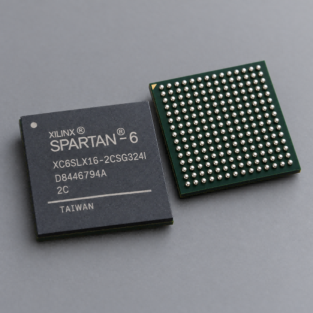
Do the Power and Voltage Requirements Match Your System?
The board must support the core, auxiliary, and I/O-bank supply requirements of the FPGA. For a standard-performance -2 Spartan-6 device, VCCINT is 1.2 V nominal, with a recommended operating range of 1.14 to 1.26 V.
VCCAUX supports specified 2.5 V or 3.3 V operating ranges, while VCCO depends on the I/O standard used in each bank. This means the XC6SLX16-2CSG324I cannot be treated as a single-supply device. Different external interfaces can require different VCCO planning across the I/O banks.
Power evaluation should cover VCCINT, VCCAUX, each VCCO rail, regulator capacity, decoupling, startup conditions, and expected operating power. If the device is being considered for an existing board, verify the existing power tree early. A different core-voltage variant or incompatible I/O-bank voltage can rule out an otherwise similar FPGA before timing analysis is necessary.
What Clocking and Configuration Requirements Should You Verify?
Confirm that the available clock inputs and clock-management resources can support every required clock domain, and decide how the FPGA will load its bitstream after power-up.
XC6SLX16 provides two CMTs. Each Spartan-6 CMT contains two DCMs and one PLL, giving the device four DCMs and two PLLs in total. Count the independent input clocks, generated frequencies, phase relationships, and clock-domain crossings required by the design rather than looking only at logic utilization.
Spartan-6 uses SRAM-based configuration, so XC6SLX16-2CSG324I must load its configuration after power-up. The selected boot method affects external Flash or host circuitry, configuration pins, and board connections. The configuration guide lists approximately 3.6 Mb of configuration data for XC6SLX16, which is also relevant when sizing external configuration memory.
The development environment deserves the same attention. AMD states that Vivado supports devices starting with the 7 Series, while older devices such as Spartan-6 continue to use ISE. For a legacy product this may already be part of the established workflow; for a new project, tool maintenance should be considered before the FPGA is selected.
Which XC6SLX16-2CSG324I Specifications Can Affect Your Final Device Choice?
Resource headroom, I/O compatibility, timing margin, package constraints, power architecture, external-memory needs, and missing hard features are the factors most likely to change the final choice. One serious mismatch can be enough to rule out the device.
For example, a design may fit within 14,579 logic cells but need more Block RAM or DSP resources. Another may fit internally but require an I/O combination that cannot be assigned across the four banks at the required voltages. A third may meet resource and pin requirements but fail timing on the -2 speed grade.
Architecture can be decisive as well. XC6SLX16 is an LX device with no GTP transceivers and no integrated PCIe endpoint block. If a product requires hard multi-gigabit serial links or a hard PCIe endpoint, additional logic capacity will not compensate for the missing hardware.
For an established Spartan-6 product, the XC6SLX16-2CSG324I may still fit the existing architecture and development environment well. For a new design, the ISE-based tool flow and future migration plan deserve more weight alongside the raw FPGA resources.
What Should You Confirm Before Finalizing the XC6SLX16-2CSG324I Selection?
Confirm the exact ordering code, implementation results, timing, pinout, power rails, clock architecture, configuration method, and tool flow before fixing XC6SLX16-2CSG324I in the BOM.
- Exact OPN: Keep XC6SLX16-2CSG324I intact, including -2, CSG324, and I.
- Resource fit: Review logic, Block RAM, DSP48A1, MCB, I/O, and routing use after implementation.
- Timing: Confirm that the real design closes timing on the -2 device.
- Pinout: Verify I/O banks, differential pairs, clocks, VREF, configuration pins, power, and ground.
- Power: Confirm VCCINT, VCCAUX, every required VCCO rail, regulator capacity, and startup conditions.
- Clocking: Make sure every required clock domain can use the available pins and clock resources.
- Configuration: Confirm boot mode, configuration-memory capacity, and external circuitry.
- Tool flow: Make sure the project can be built and maintained with the required Spartan-6 ISE environment.
AMD states that formal support for Spartan-6, including all speed and temperature grades, has been extended through at least 2030. That helps with lifecycle planning, but exact package, date-code, and lot availability should still be checked when procurement begins.
Once engineering has qualified the device, purchasing should continue using the complete ordering code instead of shortening it to XC6SLX16. This reduces the risk of changing the speed grade, package, or temperature grade between design approval and ordering.
FAQs About XC6SLX16-2CSG324I
Q1. Can XC6SLX16-2CSG324I be used in Vivado?
A1. No. Spartan-6 uses the Xilinx ISE tool flow rather than Vivado. AMD states that Vivado device support starts with the 7 Series. This is also a recurring practical issue among engineers maintaining Spartan-6 projects on newer development machines.
Q2. How much configuration memory does XC6SLX16 need?
A2. The Spartan-6 configuration guide lists approximately 3.6 Mb for an XC6SLX16 configuration image. If the Flash must also hold multiple FPGA images or application data, leave additional capacity rather than sizing it exactly to the bitstream.
Q3. Can XC6SLX16-2CSG324I boot without a JTAG programmer connected?
A3. Yes. JTAG is useful during programming and development, but normal standalone operation can load the FPGA from a supported external configuration source. The boot mode and configuration wiring must be designed correctly.
Q4. Can the configuration Flash also store other system data?
A4. Yes, provided the capacity and post-configuration access scheme are designed for it. Reserve enough memory for the required FPGA image or images before allocating space to other nonvolatile data.
Q5. Can a -1L Spartan-6 device replace the -2 part without changing the power design?
A5. Do not assume so. Standard-performance -2 devices use a 1.2 V nominal VCCINT, while -1L devices use a lower VCCINT range. The power tree and timing requirements therefore need to be checked before considering that substitution.
Q6. Can any newer SPI Flash replace the original configuration Flash?
A6. Not automatically. Electrical and boot-protocol compatibility are only part of the check; legacy programming tools may also depend on recognized Flash manufacturer and device IDs. Spartan-6 users have reported cases where a Flash can work electrically but is not directly recognized by the programming flow.
Q7. Does XC6SLX16-2CSG324I require external DDR memory?
A7. No. XC6SLX16 already provides 576 Kb of Block RAM plus distributed RAM. External DDR, DDR2, DDR3, or LPDDR is needed only when the application requires more memory or a different memory architecture.
Q8. Can the same PCB footprint be reused when moving to another Spartan-6 density?
A8. Sometimes, but only for compatible device/package migration combinations. Always compare the exact pinout, power pins, special-function pins, available I/O, and required configuration-memory capacity before treating another Spartan-6 device as footprint-compatible. AMD’s configuration guide specifically discusses density migration and the change in configuration-memory size between devices such as XC6SLX9 and XC6SLX16.
Q9. Which documents should be checked besides the XC6SLX16-2CSG324I datasheet?
A9. Use the Spartan-6 Family Overview, DC and Switching Characteristics, Packaging and Pinout specification, Configuration User Guide, SelectIO documentation, and the Memory Controller Block guide when external memory is used. A single device overview cannot provide every pin, electrical, configuration, and memory-interface detail required for final board design.
Q10. Is XC6SLX16-2CSG324I still suitable for a long-life product?
A10. AMD has extended Spartan-6 support through at least 2030. For a long-life product, also evaluate the exact package and speed-grade supply requirements, toolchain maintenance, configuration-memory sourcing, and whether a future migration path should be planned.
If XC6SLX16-2CSG324I is already qualified for your design, send the required quantity, date code requirement, and delivery location to sales@melsonchip.com. Melson Components can align the supplied device with the agreed OPN, packaging, traceability, and inspection requirements before shipment.
For projects that require additional verification, inspection can be arranged according to the agreed scope, including visual inspection, X-Ray, De-Cap, or functional testing where appropriate. This keeps the purchasing check tied to the same device specification that engineering approved.